

Zigzag Pattern for TSV Copper Adhesion
a technology of tsv copper and adhesion pattern, which is applied in the direction of semiconductor devices, semiconductor/solid-state device details, electrical apparatus, etc., can solve the problems of limiting the thermal budget of later processes, undesirable restriction on subsequent process conditions, and low adhesion of copper conductors to underlying materials, etc., to achieve better adhesion, more process flexibility, and better adhesion
- Summary
- Abstract
- Description
- Claims
- Application Information
AI Technical Summary
Benefits of technology
Problems solved by technology
Method used
Image

Examples
Embodiment Construction
[0023]The making and using of the presently preferred embodiments are discussed in detail below. It should be appreciated, however, that the present invention provides many applicable inventive concepts that can be embodied in a wide variety of specific contexts. The specific embodiments discussed are merely illustrative of specific ways to make and use the invention, and do not limit the scope of the invention.
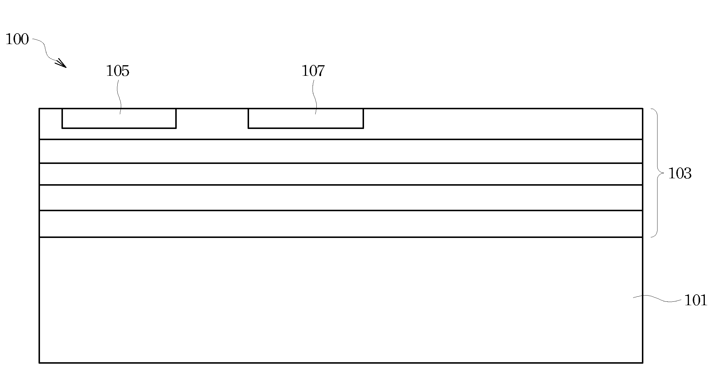
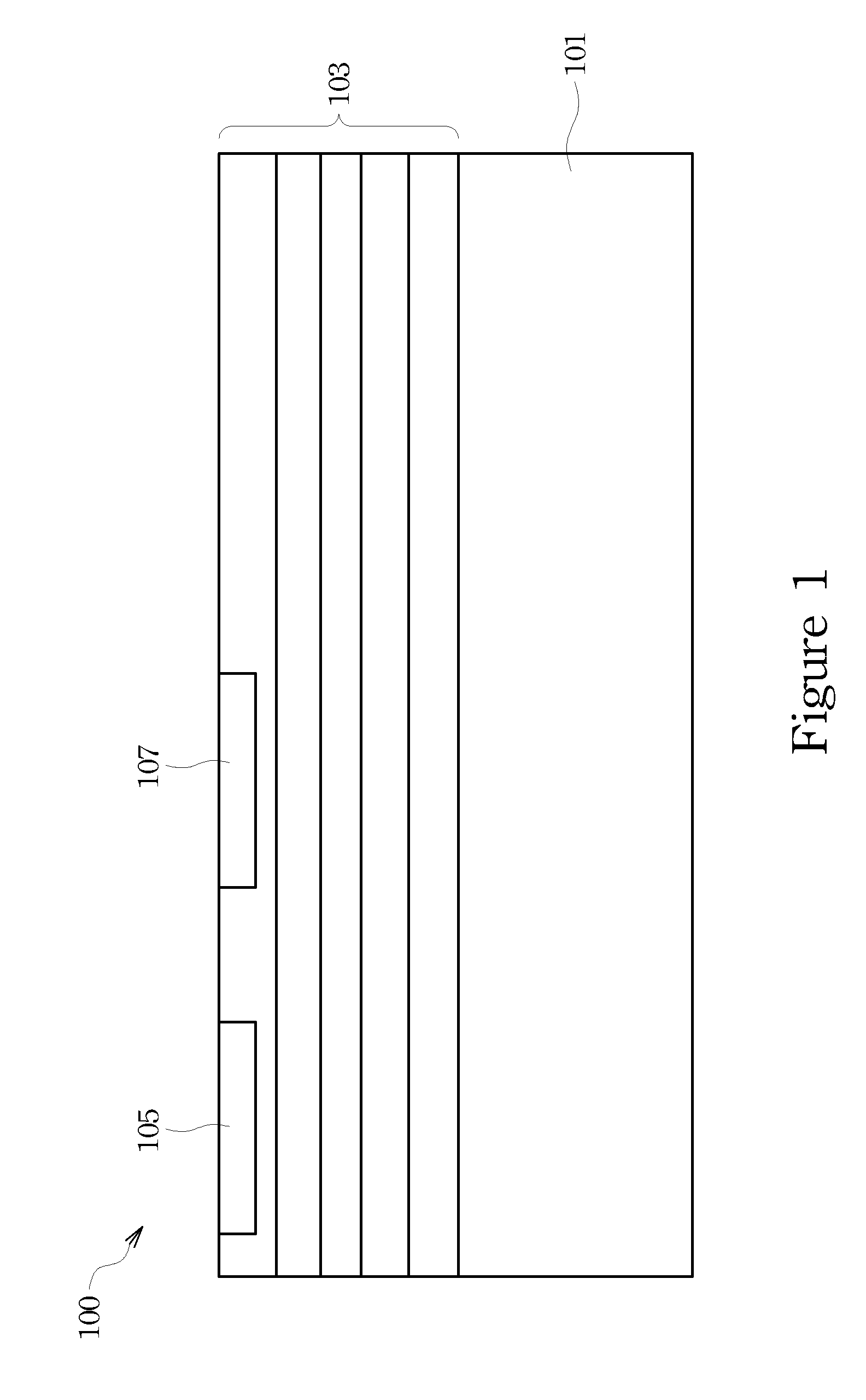
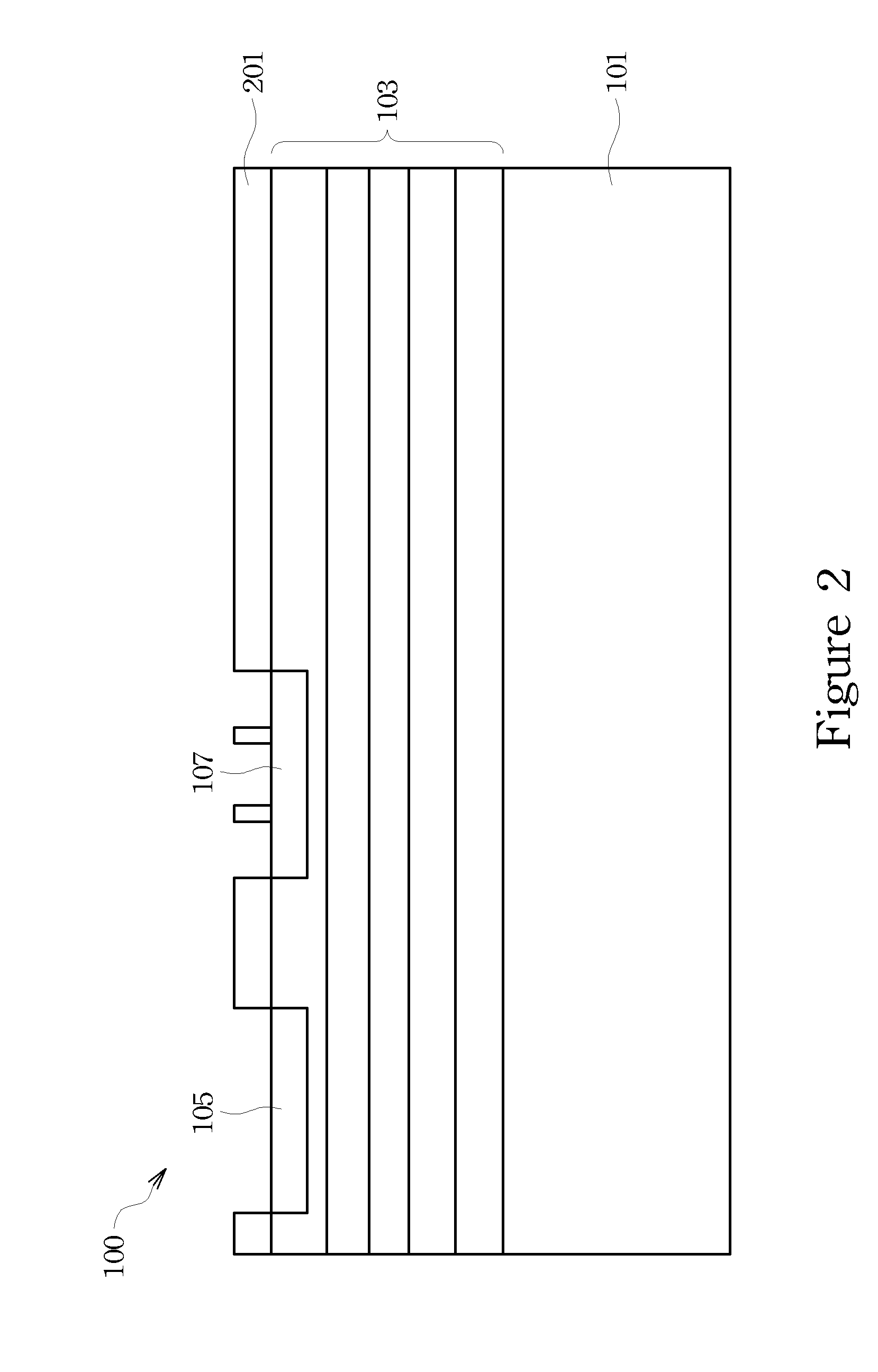
[0024]The present invention will be described with respect to preferred embodiments in a specific context, namely a contact pad between a metal layer and a TSV. The invention may also be applied, however, to other contact pads.
[0025]With reference now to FIG. 1, there is shown a cross-sectional view of a semiconductor die 100 comprising a substrate 101, metallization layers 103, a first upper metal contact 105, and a second upper metal contact 107. The substrate 101 may comprise bulk silicon, doped or undoped, or an active layer of a silicon-on-insulator (SOI) substrate. Gene...
PUM
 Abstract
Description
Claims
Application Information