Thin foil for use in packaging integrated circuits

a technology of integrated circuits and thin foils, applied in the direction of transportation and packaging, manufacturing tools, and so on, can solve the problems of high cost of structure, high cost of foil based packaging processes, and inability to achieve widespread acceptance in the industry, so as to reduce heat-induced warpage in the foil and minimize warpage

Inactive Publication Date: 2010-04-08
NAT SEMICON CORP
View PDF16 Cites 32 Cited by
  • Summary
  • Abstract
  • Description
  • Claims
  • Application Information

AI Technical Summary

Benefits of technology

[0007]In one aspect of the present invention, methods for minimizing warpage in a thin foil used in integrated circuit packaging are described. Portions of a metallic foil are ultrasonically welded to a carrier to form a foil carrier structure. The ultrasonic welding helps define a panel in the metallic foil that is suitable for packaging integrated circuits. One embodiment of the present invention involves forming an intermittent welding pattern that extends along the edges of the panel. In another implementation, notches and / or slots are cut in the foil carrier structure. In still another embodiment of the present invention, the materials for the metallic foil and the carrier are selected to have similar coefficients of thermal expansion. Additionally, the thicknesses of the metallic foil and the carrier may be selectively correlated to reduce heat-induced warpage in the foil.

Problems solved by technology
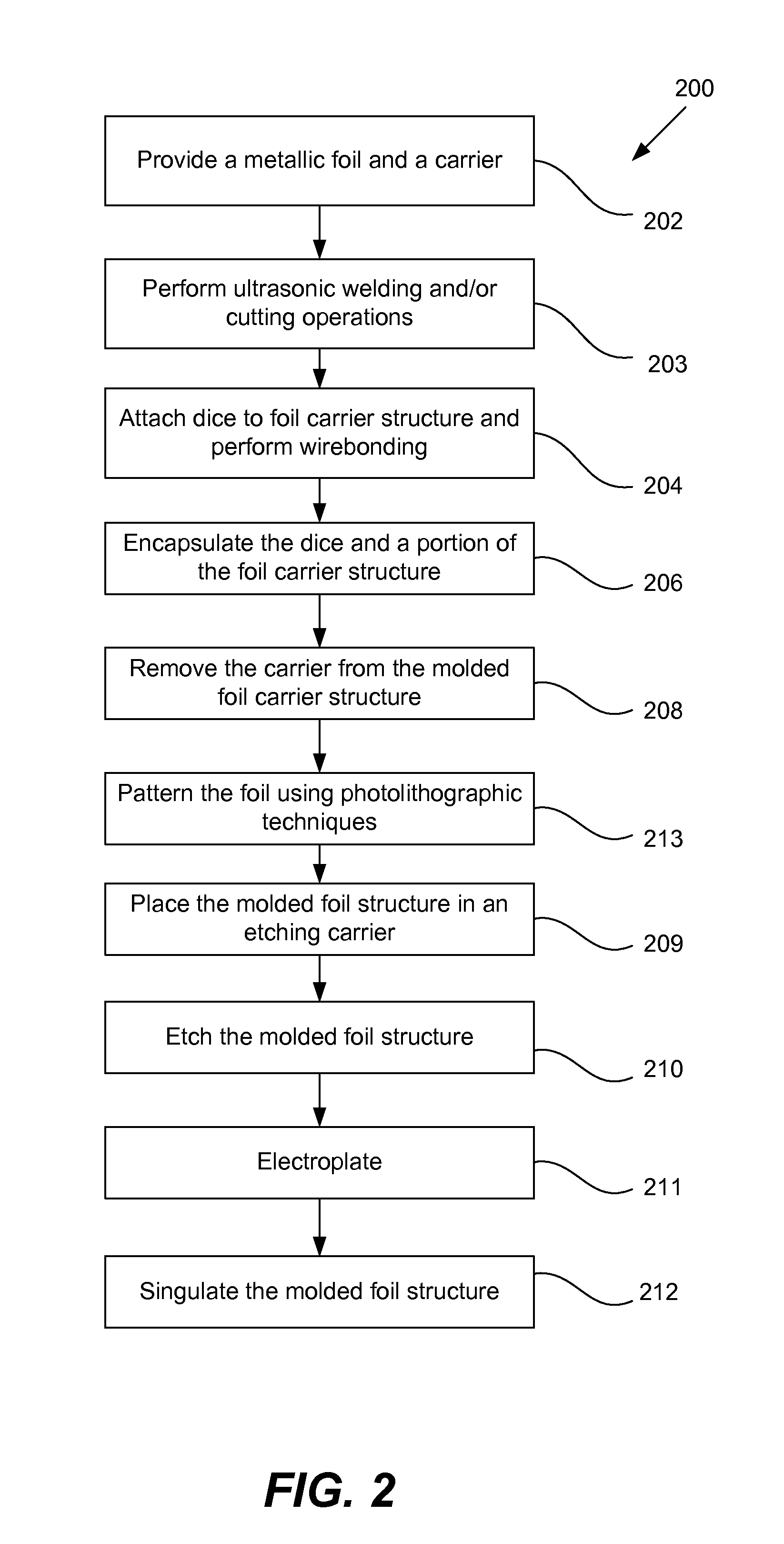
Such structures, however, may entail higher costs.
Although a number of foil based designs have been developed, none have achieved widespread acceptance in the industry in part because foil based packaging processes tend to be more expensive than conventional leadframe packaging and in part because much of the existing packaging equipment is not well suited for use with such foil based package designs.

Method used


Image

  • Thin foil for use in packaging integrated circuits
  • Thin foil for use in packaging integrated circuits
  • Thin foil for use in packaging integrated circuits

Examples


Embodiment Construction

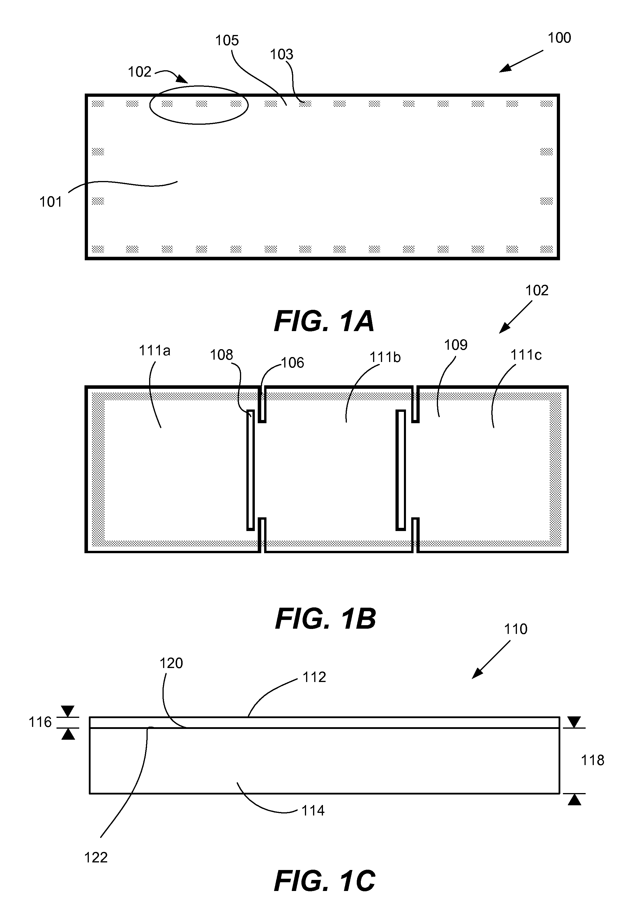
[0024]The present invention relates generally to the packaging of integrated circuits using thin foils. Various approaches for incorporating thin foils into integrated circuit packaging involve welding a thin foil to a carrier to form a foil carrier structure. At various stages in the packaging and assembly process (e.g., die attach cure, wire bonding, molding, etc.), the foil carrier structure is subjected to high temperatures. Generally, since the carrier and the foil are welded together, temperature cycling can cause frame warpage due to the CTE mismatch between the carrier and the foil, which may cause problems during package assembly and degrade the performance and reliability of the resulting integrated circuit package. Although pressure can be applied to the thin foil to arrest warpage, this generally requires additional process steps and / or materials. Accordingly, the present invention pertains to arrangements and methods for reducing warpage while minimizing or eliminating ...


PUM

PropertyMeasurementUnit
thicknessaaaaaaaaaa
thicknessaaaaaaaaaa
thicknessaaaaaaaaaa

Abstract

Methods for minimizing warpage of a welded foil carrier structure used in the packaging of integrated circuits are described. Portions of a metallic foil are ultrasonically welded to a carrier to form a foil carrier structure. The ultrasonic welding helps define a panel in the metallic foil that is suitable for packaging integrated circuits. Warpage of the thin foil can be limited in various ways. By way of example, an intermittent welding pattern that extends along the edges of the panel may be formed. Slots may be cut to define sections in the foil carrier structure. Materials for the metallic foil and the carrier may be selected to have similar coefficients of thermal expansion. An appropriate thickness for the metallic foil and the carrier may be selected, such that the warpage of the welded foil carrier structure is limited when the foil carrier structure is subjected to large increases in temperature. Foil carrier structures for use in the above methods are also described.

Description

CROSS-REFERENCE TO RELATED APPLICATIONS[0001]This application is a Continuation-in-Part of and claims priority to U.S. patent application Ser. No. 12 / 133,335, entitled “Foil Based Semiconductor Package,” filed Jun. 4, 2008, which is hereby incorporated by reference in its entirety for all purposes.TECHNICAL FIELD[0002]The present invention relates generally to the packaging of integrated circuits. More particularly, the present invention relates to packaging methods and arrangements involving thin foils.BACKGROUND OF THE INVENTION[0003]There are a number of conventional processes for packaging integrated circuit (IC) dice. By way of example, many IC packages utilize a metallic leadframe that has been stamped or etched from a metal sheet to provide electrical interconnects to external devices. The die may be electrically connected to the leadframe by means of bonding wires, solder bumps or other suitable electrical connections. In general, the die and portions of the leadframe are en...

Claims


Application Information

Patent Timeline
Patent Type & Authority Applications(United States)
IPC IPC(8): H01L23/48B32B15/04B32B3/00B23K1/06H01L21/50
CPCH01L21/4832Y10T428/24612H01L21/6835H01L23/3107H01L23/49582H01L23/544H01L24/85H01L24/97H01L2221/68345H01L2223/5442H01L2223/54426H01L2223/54473H01L2224/48091H01L2224/97H01L2924/01013H01L2924/01029H01L2924/01046H01L2924/01082H01L2924/14H01L2924/3511H05K3/025H05K3/328H05K2203/0152H01L21/568H01L2224/85H01L2924/014H01L2924/01033H01L24/48H01L2924/01006H01L2924/00014H01L2924/181Y10T428/31678H01L2924/00012H01L2224/45099H01L2224/45015H01L2924/207
Inventor PODDAR, ANINDYABAYAN, JAIME A.TU, NGHIA THUCWONG, WILL K.PHAM, KEN
Owner NAT SEMICON CORP
Why Eureka
Try Eureka