
Reflective semiconductor optical amplifier and optical signal processing method using the same

a semiconductor optical amplifier and optical signal processing technology, applied in semiconductor lasers, multiplex communication, active medium materials, etc., can solve the problems of high optical cost, ld) is required, and price competitive wdm-pon may be difficult to realize, and achieve the effect of high operating speed and low cos

Inactive Publication Date: 2010-04-15
ELECTRONICS & TELECOMM RES INST
View PDF40 Cites 14 Cited by
  • Summary
  • Abstract
  • Description
  • Claims
  • Application Information

AI Technical Summary

Benefits of technology

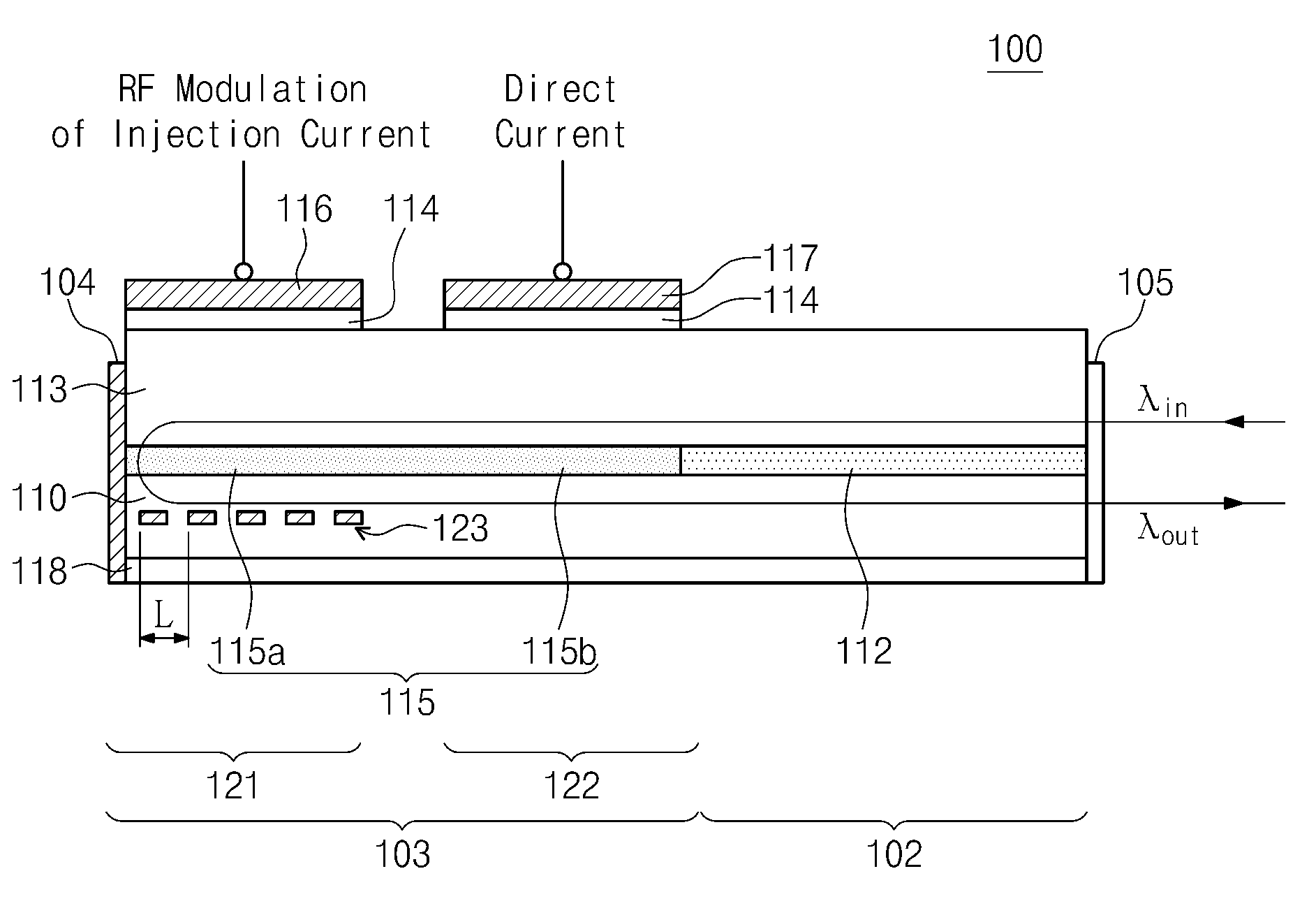
[0007]The present invention provides an inexpensive and high operating speed reflective semiconductor amplifier.

Problems solved by technology

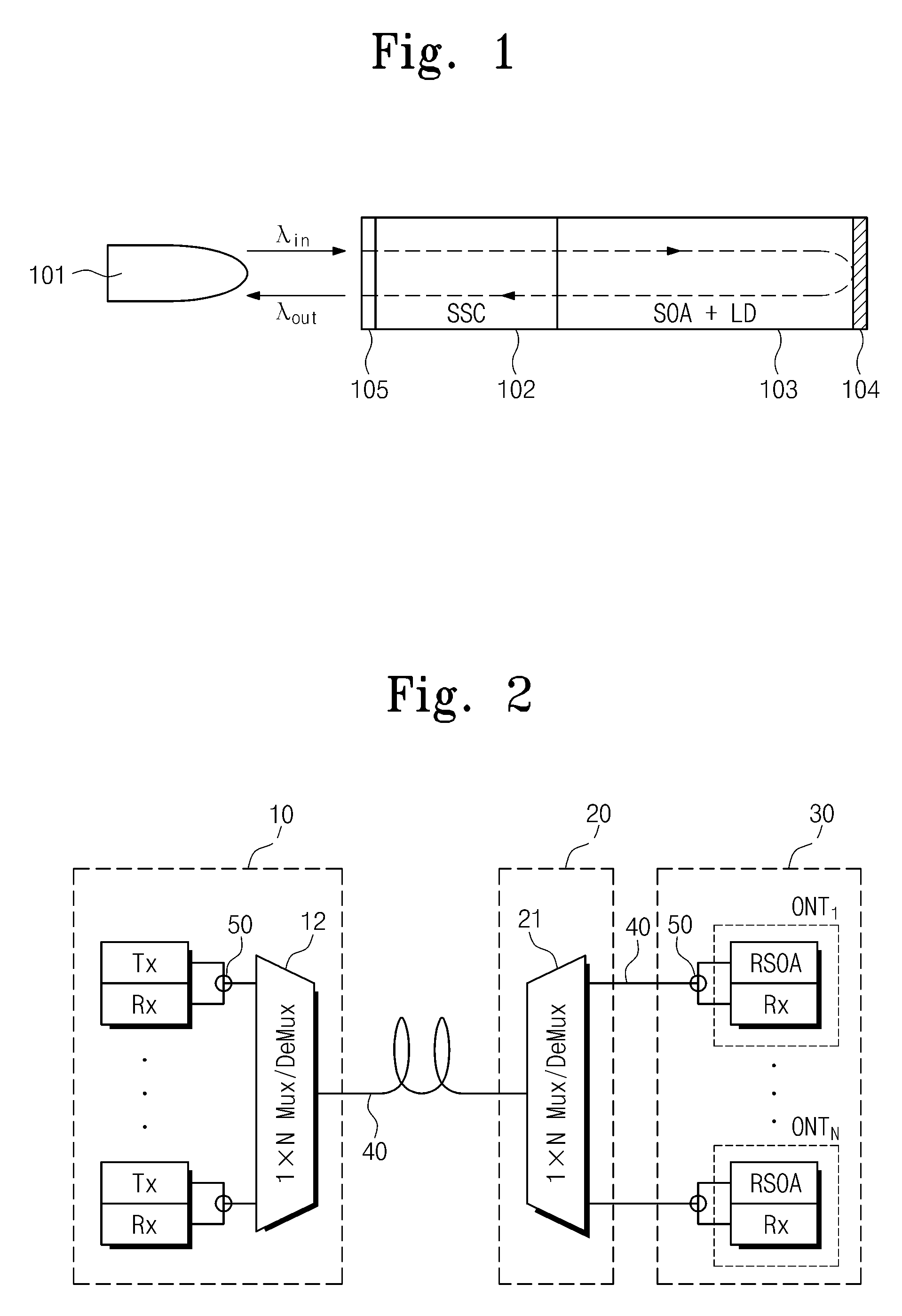
However, according to the WDM-PON, a very expensive optical source such as Distributed Feedback Laser Diode (DFB-LD) is required for each subscriber to use respectively different wavelengths.
That is, if a wavelength dependable optical source is used, a price competitive WDM-PON may be difficult to realize.

Method used


Image

  • Reflective semiconductor optical amplifier and optical signal processing method using the same
  • Reflective semiconductor optical amplifier and optical signal processing method using the same
  • Reflective semiconductor optical amplifier and optical signal processing method using the same

Examples


Embodiment Construction

[0033]Preferred embodiments of the present invention will be described below in more detail with reference to the accompanying drawings. The present invention may, however, be embodied in different forms and should not be construed as limited to the embodiments set forth herein. Rather, these embodiments are provided so that this disclosure will be thorough and complete, and will fully convey the scope of the present invention to those skilled in the art.

[0034]In the specification, it will be understood that when a layer (or film) is referred to as being ‘on’ another layer or substrate, it can be directly on the other layer or substrate, or intervening layers may also be present. Also, in the figures, the dimensions of layers and regions are exaggerated for clarity of illustration. Also, though terms like a first, a second, and a third are used to describe various regions and layers in various embodiments of the present invention, the regions and the layers are not limited to these ...


PUM


Abstract

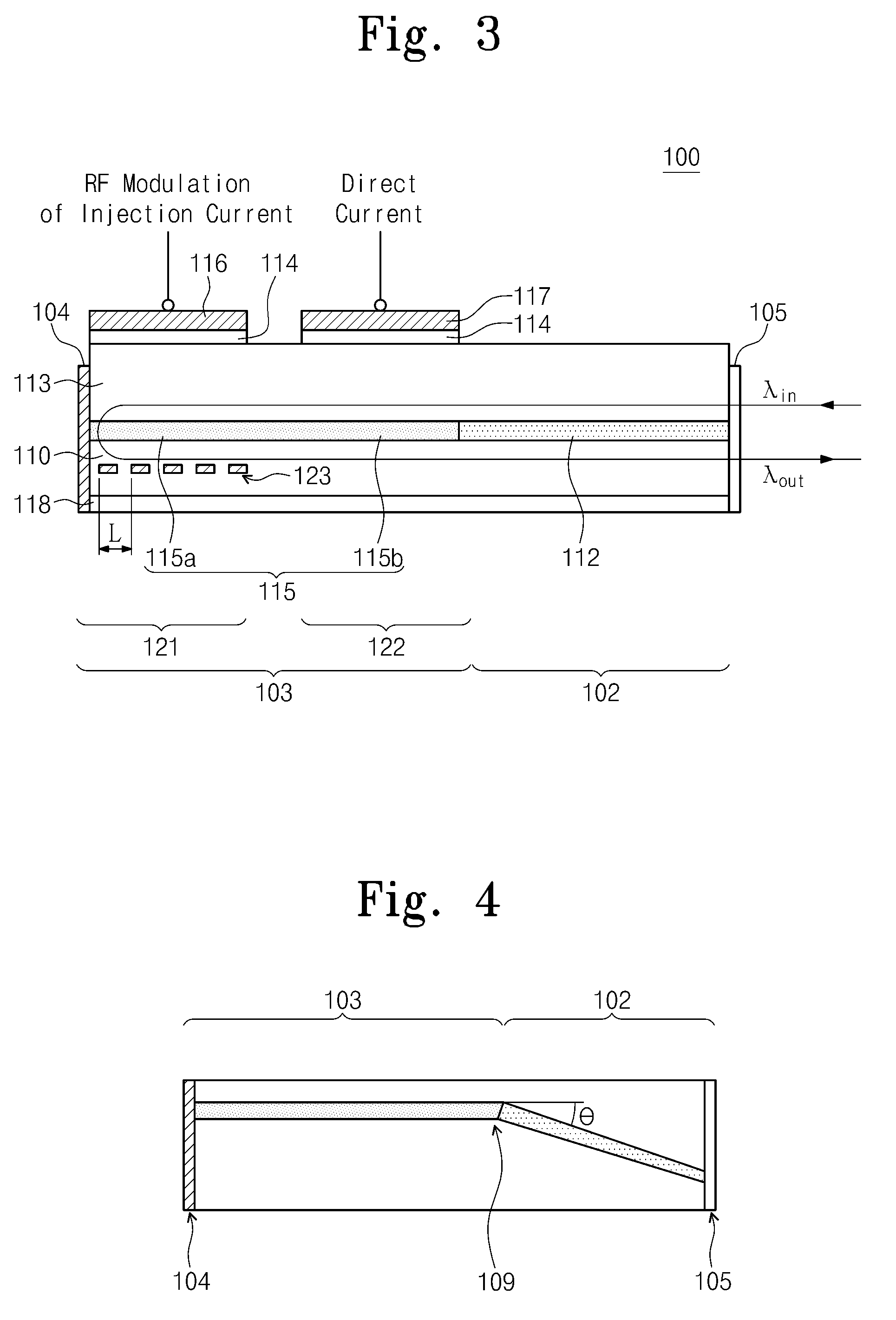
Provided are a semiconductor optical amplifier and an optical signal processing method using the same. The reflective semiconductor optical amplifier includes: an optical signal amplification region operating to allow a downward optical signal incident from the external to obtain a gain; and an optical signal modulation region connected to the optical signal amplification region and generating a modulated optical signal. The downward optical signal is amplified through a cross gain modulation using the modulated optical signal and is outputted as an upward optical signal.

Description

CROSS-REFERENCE TO RELATED APPLICATIONS[0001]This U.S. non-provisional patent application claims priority under 35 U.S.C. §119 of Korean Patent Application No. 10-2008-0099613, filed on Oct. 10, 2008, the entire contents of which are hereby incorporated by reference.BACKGROUND OF THE INVENTION[0002]The present invention disclosed herein relates to a semiconductor optical amplifier and an optical signal processing method using the same, and more particularly, to a semiconductor optical amplifier using a cross gain modulation and an optical signal processing method using the same.[0003]As high speed internet and diverse multimedia services are introduced lately, Fiber To The Home (FTTH) technology for connecting a telephone station to a home through an optical fiber has been actively developed in order to provide a large amount of information to a user. To commercially use this technology, it is necessary to transmit a large amount of information and achieve a low cost for realizing i...

Claims


Application Information

Patent Timeline
IPC IPC(8): H04J14/02H01S3/16
CPCH01S5/026H01S5/0608H01S5/509H01S5/1014H01S5/50H01S5/06258H01S3/16H04B10/00H04B10/291
Inventor KIM, HYUN SOOKWON, O-KYUNKIM, DONG CHURLCHOI, BYUNG-SEOKKIM, KISOOOH, DAE KON
Owner ELECTRONICS & TELECOMM RES INST
Learn More