Solar cell with nanostructure electrode(s)

a nano-structure, solar cell technology, applied in the field of thin-film solar cells, can solve the problems of high cost of c-, severe damage to the underlying active layer, and the indium component of ito is rapidly becoming a scarce commodity, and achieves the effect of high power conversion efficiency

Inactive Publication Date: 2010-04-22
UNIDYM
View PDF6 Cites 62 Cited by
  • Summary
  • Abstract
  • Description
  • Claims
  • Application Information

AI Technical Summary

Benefits of technology

[0016]In a yet further embodiment, a solar cell according to the present invention may also comprise a second active layer sandwiched between a third electrode and the first or second electrode. Preferably, at least two of the first, second and third electrodes are at least semi-transparent to allow light transmission through to the multiple active layers. If the third electrode serves as a cathode, it may require a third buffer layer (e.g., a hole blocking layer with a low work function). In this way, transparent solar cells (e.g., thin-film solar cells) with different spectral responses may be stacked together with intervening at least semi-transparent electrodes (e.g., comprising nanostructure networks) to achieve high power conversion efficiency.

Problems solved by technology

However, the high cost of c-Si wafers has led the industry to research alternate, and generally less-expensive, solar cell materials.
However, ITO can be an inadequate solution for many emerging applications (e.g., non-rigid solar cells due to ITO's brittle nature), and the indium component of ITO is rapidly becoming a scarce commodity.
Moreover, deposition of transparent conducting oxides (TCOs) for minimal light loss normally requires a sputtering process, which can severely damage underlying active layers.

Method used


Image

  • Solar cell with nanostructure electrode(s)
  • Solar cell with nanostructure electrode(s)
  • Solar cell with nanostructure electrode(s)

Examples


example

Solar Cell With Electrode Grid

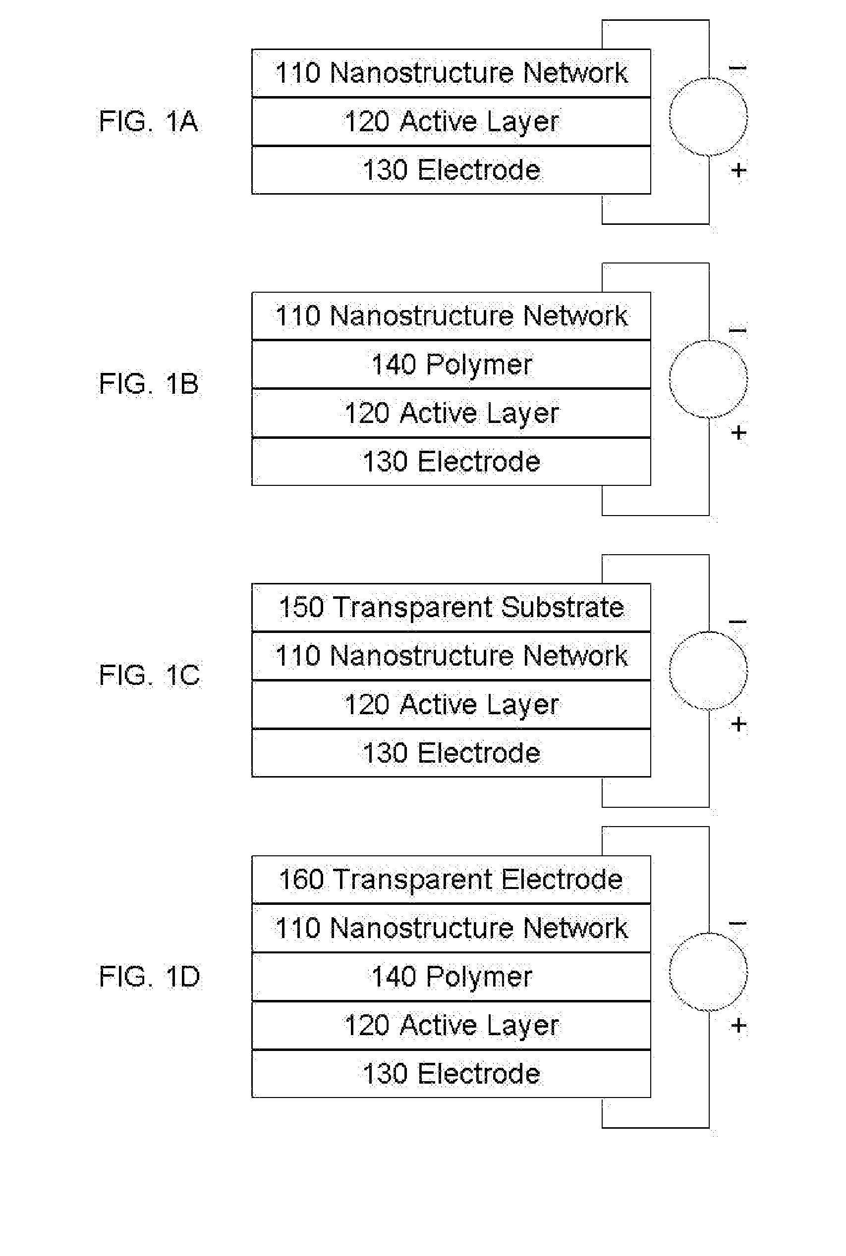
[0053]In a solar cell, incoming light separates charges in a photosensitive active layer 120. However, these separated charges usually cannot travel far within this usually-thin functional layer before recombining.

[0054]Electrodes in an electrode grid 510 can gather these separated charges, but only if the charges can reach points in the active layer 120 that contact the electrodes 510. Unfortunately, these electrodes 510 must be spaced relatively far apart in a conventional metal electrode grid, given that the non-transparent electrodes thereof reduce light transmission to the underlying active layer 120 (the reduction in light transmission is proportional to the fractional area covered by the non-transparent electrodes of the metal electrode grid 510). Semi-transparent electrodes can be more closely spaced, however without an additional transparent conductive layer(s), a solar cell having only an electrode grid may nonetheless have low efficiency.

[005...


PUM

PropertyMeasurementUnit
sheet resistanceaaaaaaaaaa
semi-transparentaaaaaaaaaa
sheet resistancesaaaaaaaaaa

Abstract

A solar cell comprising at least one nanostructure-film electrode is discussed. The solar cell may further comprise a different conducting material, such as a conducting polymer, to fill pores in the nanostructure-film. Additionally or alternatively, the solar cell may comprise an electrode grid superimposed on the nanostructure-film. Likewise, the solar cell may have a single or multiple active layer(s), wherein nanostructure-film(s) may form at least semi-transparent anode(s) and/or cathode(s) through use of buffer layer(s).

Description

COPYRIGHT & TRADEMARK NOTICE[0001]A portion of the disclosure of this patent document contains material that is subject to copyright protection. The owner has no objection to the facsimile reproduction by any one of the patent document or the patent disclosure, as it appears in the Patent and Trademark Office patent file or records, but otherwise reserves all copyrights whatsoever.[0002]Certain marks referenced herein may be common law or registered trademarks of third parties affiliated or unaffiliated with the applicant or the assignee. Use of these marks is by way of example and shall not be construed as descriptive or limit the scope of this invention to material associated only with such marks.FIELD OF THE INVENTION[0003]The present invention relates in general to solar cells, and more particularly to thin-film solar cells comprising at least one nanostructure-film.BACKGROUND OF THE INVENTION[0004]A solar cell is a photoelectric device that converts photons from the sun (solar ...

Claims


Application Information

Patent Timeline
Patent Type & Authority Applications(United States)
IPC IPC(8): H01L31/00H01L33/00H01L51/42H01L51/50
CPCB82Y20/00H01L31/022425H01L31/022466H01L51/0037Y02E10/549H01L51/444H01L51/5206H01L51/5234H01L2251/5323H01L51/4253H10K85/1135H10K30/821H10K30/30H10K50/81H10K50/814H10K50/828H10K2102/3031
Inventor HU, LIANGBINGHECHT, DAVIDGRUNER, GEORGE
Owner UNIDYM
Why Eureka
Try Eureka