Thermally improved semiconductor qfn/son package

a technology of semiconductor qfn and package, which is applied in the direction of semiconductor devices, semiconductor/solid-state device details, electrical apparatus, etc., can solve the problems of reducing the risk of breaking wafers in the transportation from the wafer fab to the assembly site, poor thermal conductivity of polymers, etc., to improve qfn/son thermal performance, enhance thermal flux vertically, and optimize thermal flux

Active Publication Date: 2010-04-22
TEXAS INSTR INC
View PDF5 Cites 9 Cited by
  • Summary
  • Abstract
  • Description
  • Claims
  • Application Information

AI Technical Summary

Benefits of technology

[0014]The technical advantage of improved QFN/SON thermal performance is based on the invention's structure to optimize the thermal flux. The thermal flux Q per unit of time is equal to the product of thermal conductivity λ multiplied by the gradient of temperature T, in the direction of decreasing temperature, and by the area q perpendicular to the temperature gradient:
[0015]The invention enhances the thermal flux vertically away from the heat-generating active circuit components into the substrate heat sink by impro

Problems solved by technology

Polymers are poor thermal conductors, and their interfaces are infamous for delaminations.
Further, the tradi

Method used


Image

  • Thermally improved semiconductor qfn/son package
  • Thermally improved semiconductor qfn/son package
  • Thermally improved semiconductor qfn/son package

Examples


Embodiment Construction

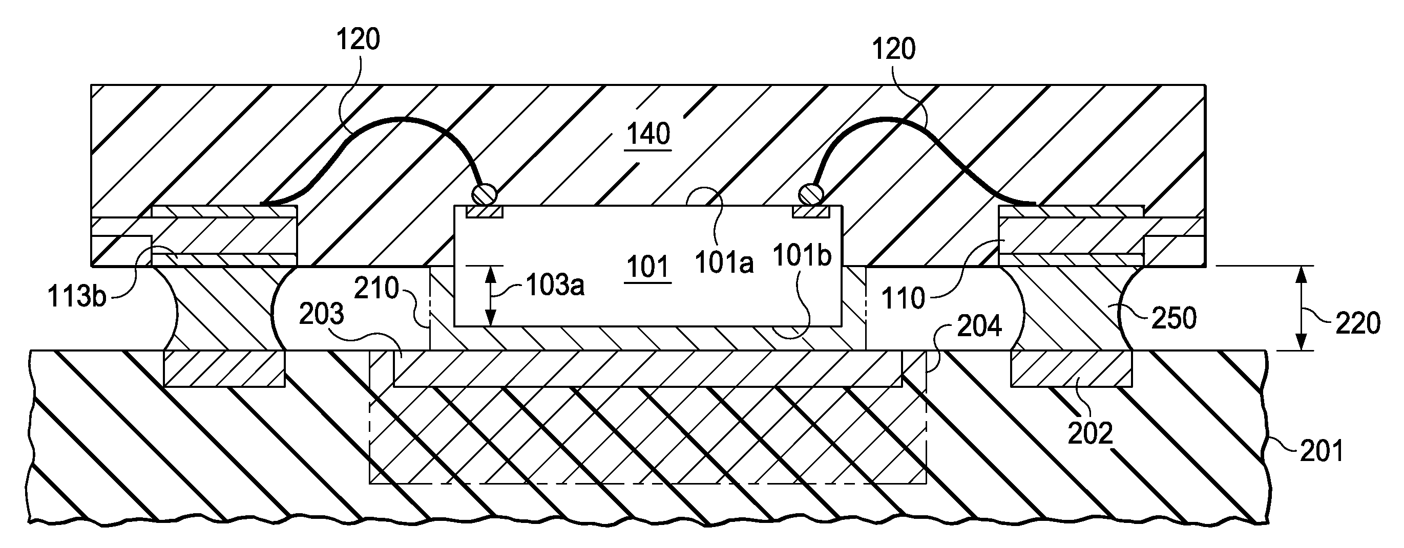
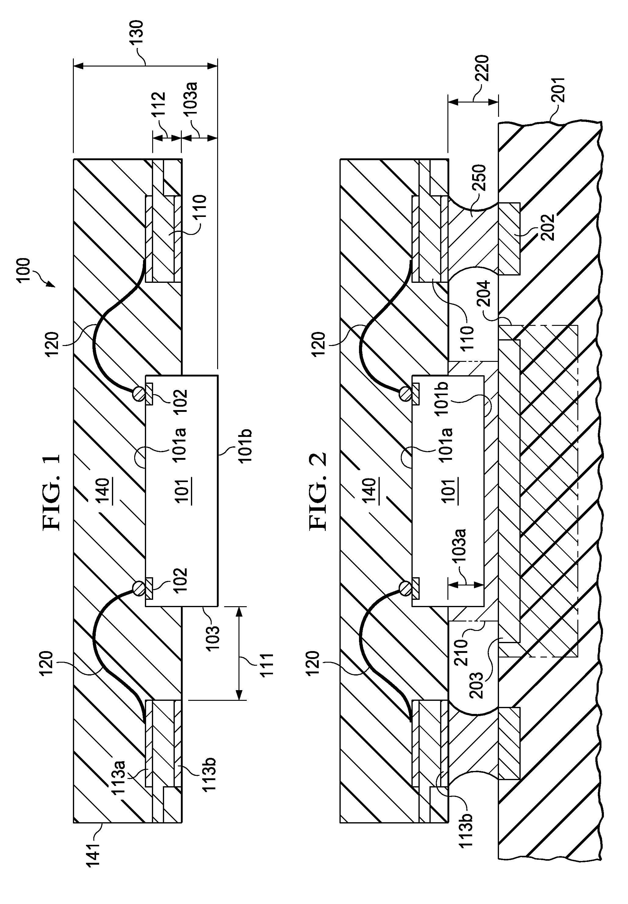
[0026]FIG. 1 (not to scale) illustrates an embodiment of the invention, generally designated 100. The Figure shows a packaged semiconductor device without cantilevered leads, which is frequently referred to as a Quad Flat No-lead (QFN) or Small-Outline No-lead (SON) device. The packaged device includes a semiconductor chip 101 with a first surface 101a and terminals 102, a second surface 101b opposite the first surface 101a, and sidewalls 103 between the surfaces. The sidewalls determine the thickness of chip 101; in the embodiment, the thickness is preferably in the range from about 225 to 350 μm.

[0027]The numerous process steps in the semiconductor integrated circuit manufacturing process flow require the robust wafer thickness of about 275 to 350 μm in order to avoid the risk of fracture during the frequent wafer handling. However, when customer applications call for a thin overall device thickness (0.55 to 1.0 mm), conventional technology requires a thin chip, necessitating a re...


PUM


Abstract

A semiconductor device without cantilevered leads uses conductive wires (120) to connect the chip terminals to the leads (110), and a package compound (140) to encapsulate the chip surface (101a) with the terminals, the wires, and the lead surfaces with the attached wires. The chip surface (101b) opposite the terminals together with portions (103) of the chip sidewalls protrude from the package, allowing an unimpeded thermal contact of the protruding chip surface to a substrate (201) to optimize the thermal flux from the chip to the substrate. Solder bodies (250) attached to the compound-free lead surfaces (113b) can be connected to the substrate so that the solder bodies are as elongated as the protruding chip height, facilitating the void-free distribution of an underfill compound into the space between chip and substrate, and improving the absorption of thermomechanical stresses during device operation.

Description

FIELD OF THE INVENTION[0001]The present invention is related in general to the field of semiconductor devices and processes, and more specifically to the structure and fabrication method of thin Quad Flat-No-lead and Small Outline No-lead semiconductor packages with outstanding thermal characteristics.DESCRIPTION OF RELATED ART[0002]A major part of the conventional package of a semiconductor device is a metallic leadframe, commonly made of a copper alloy. The leadframe serves several needs. First, it includes a pad as a stable support for positioning the chip during the assembly steps; thereafter, during device operation, the pad is expected to support thermal conduction and heat distribution. The assembly itself is typically performed by attaching the chip to the pad with an adhesive polymer material, which is later polymerized. From the standpoint of distributing the operational heat from the chip to the outside world, the polymer layer represents a barrier, since its thermal cond...

Claims


Application Information

Patent Timeline
IPC IPC(8): H01L23/495H01L21/60
CPCH01L21/568H01L21/6835H01L23/3107H01L23/49548H01L23/49582H01L24/32H01L24/45H01L24/48H01L24/97H01L2221/68372H01L2224/32057H01L2224/45015H01L2224/45144H01L2224/45147H01L2224/48091H01L2224/48247H01L2224/48465H01L2224/48599H01L2224/73265H01L2224/83101H01L2224/83191H01L2224/83385H01L2224/83894H01L2224/85001H01L2224/97H01L2924/01013H01L2924/01014H01L2924/01028H01L2924/01029H01L2924/01031H01L2924/01032H01L2924/01046H01L2924/01047H01L2924/01075H01L2924/01079H01L2924/01082H01L2924/014H01L2924/14H01L2924/18165H01L2924/20105H01L2924/20106H01L2924/20107H01L2924/20751H01L2924/20752H01L2924/20753H01L2924/01006H01L2924/01033H01L2924/01087H01L2924/10253H01L2224/48511H01L2924/00014H01L2224/85H01L2924/00012H01L2924/00H01L2924/3512H01L2924/181H01L2224/85455H01L2224/85664H01L2224/85444H01L2224/05599
Inventor ABBOTT, DONALD C.
Owner TEXAS INSTR INC
Why Eureka
Try Eureka