Vacuum channel transistor and diode emitting thermal cathode electrons, and method of manufacturing the vacuum channel transistor

a vacuum channel transistor and diode technology, applied in the field of transistors, can solve the problems of poor electrical characteristics between the anode and the cathode, unstable emitting current, and damage to the field emission device due to excessive current easily occurring, etc., to achieve stable electron emission structure, improve mass production, and low driving voltage

Inactive Publication Date: 2010-04-29
ELECTRONICS & TELECOMM RES INST
View PDF3 Cites 23 Cited by
  • Summary
  • Abstract
  • Description
  • Claims
  • Application Information

AI Technical Summary

Benefits of technology

[0008]The present invention provides a vacuum channel transistor that emits thermal cathode electrons, provides a stable electron emission structure, has a low driving voltage, and improves mass production, a diode, and a method of manufacturing the vacuum channel transistor.

Problems solved by technology

However, due to a characteristic of the field emission devices in which electrons cut through the sharp surface of the cathode, electrical characteristics thereof are unstable, the uniformity of the electrical characteristics between the anode and the cathode is poor, and damage to the field emission devices due to excessive current may easily occur.
For example, since the conventional field emission devices generally employ a sharp cathode tip structure, instability of emitting current, low efficiency, short life time, and low mass production may exist due to degradation of the tip in the cathode tip structure.

Method used


Image

  • Vacuum channel transistor and diode emitting thermal cathode electrons, and method of manufacturing the vacuum channel transistor
  • Vacuum channel transistor and diode emitting thermal cathode electrons, and method of manufacturing the vacuum channel transistor
  • Vacuum channel transistor and diode emitting thermal cathode electrons, and method of manufacturing the vacuum channel transistor

Examples


Embodiment Construction

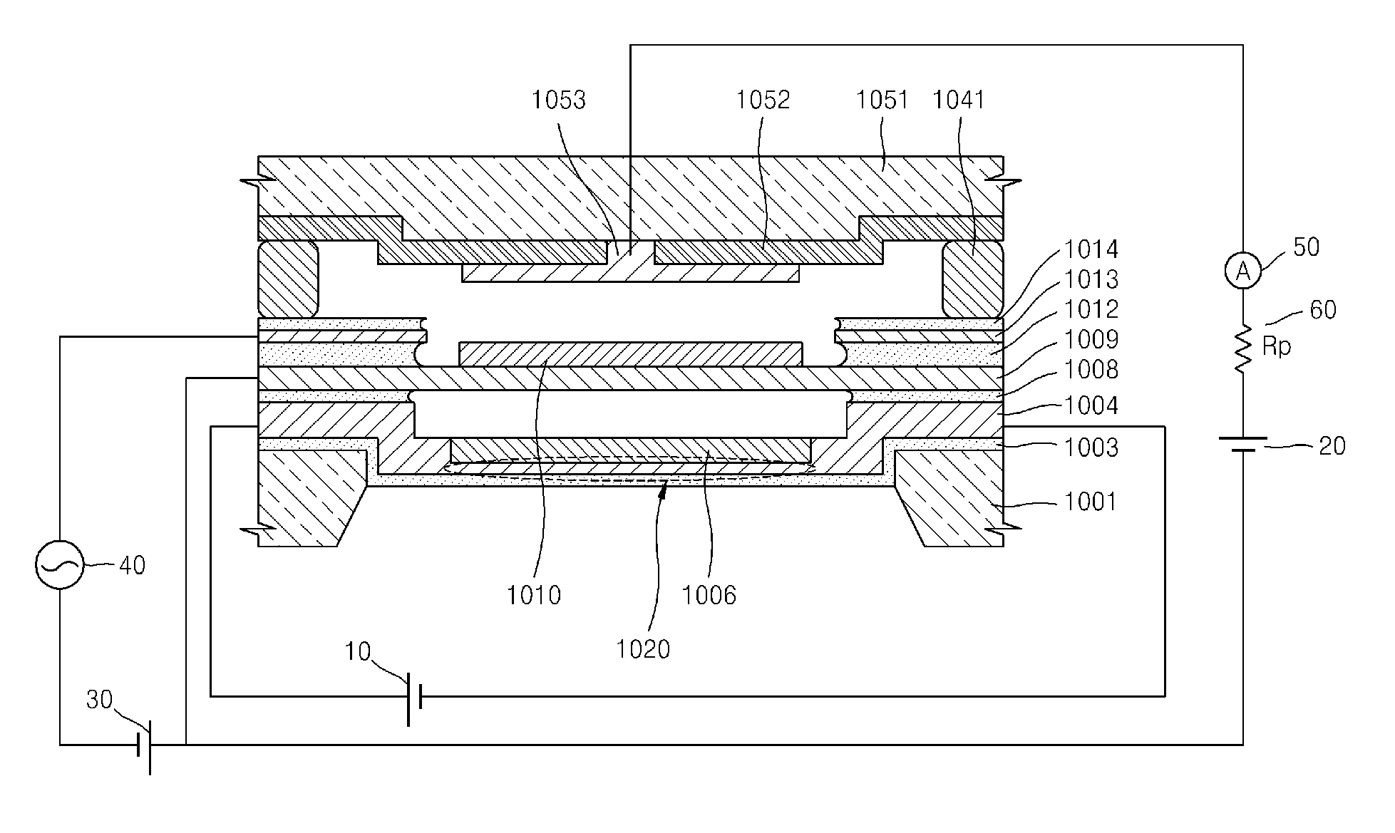
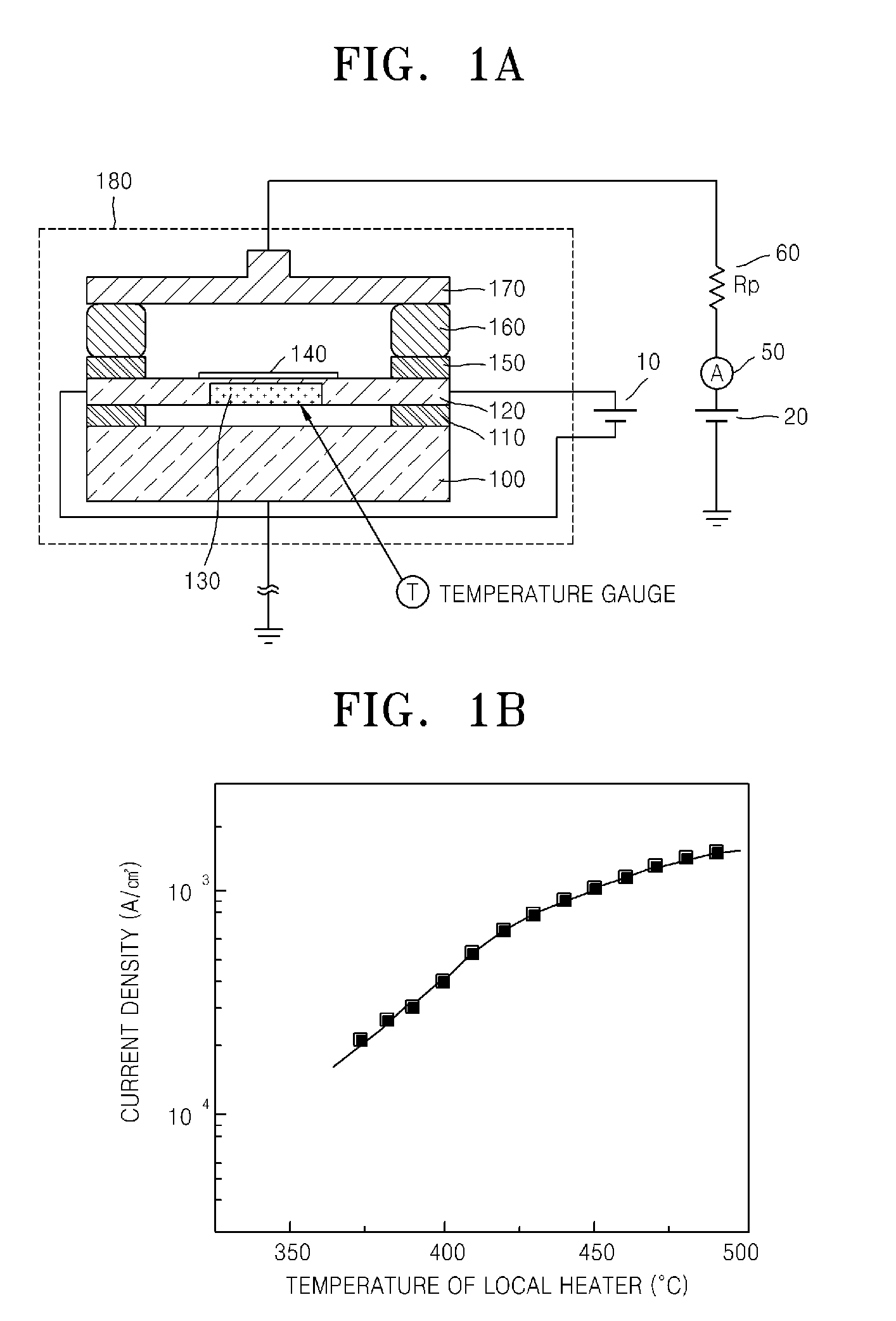
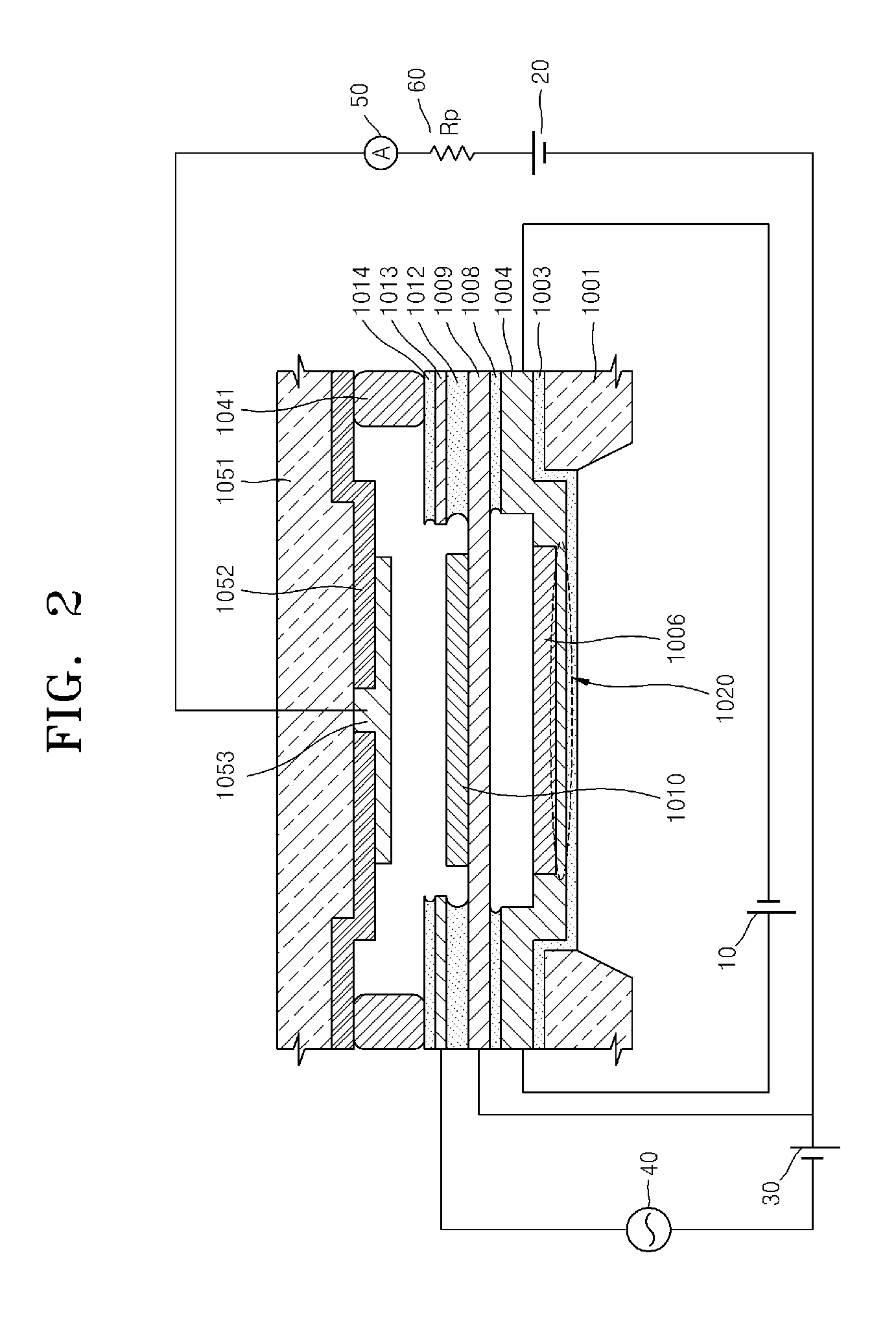
[0030]The present invention will now be described more fully with reference to the accompanying drawings, in which exemplary embodiments of the invention are shown. In the description, when it is described that an element is disposed on another element, the element may be directly disposed on the other element or a third element may be interposed therebetween. In the drawings, the thicknesses of layers and regions are exaggerated for clarity. Like reference numerals in the drawings denote like elements. The terminology used herein is for the purpose of describing exemplary embodiments only and is not intended to be limiting of example embodiments. In the description, the detailed descriptions of well-known technologies and structures may be omitted so as not to hinder the understanding of the present invention.

[0031]Thermionic emission is a method of generating free electrons and has been widely studied. According to the classical literature [W. B. Nottingham, Thermionic Emission In...


PUM


Abstract

Provided are a transistor and a method of manufacturing the transistor, and more particularly, a vacuum channel transistor emitting thermal cathode electrons and a method of manufacturing the vacuum channel transistor. The vacuum channel transistor includes: a motherboard; a micro heater member having a thin-film structure formed on the motherboard; a cathode member having a thin-film structure spaced apart from a center part of the micro heater member by a first interval and formed on the micro heater member; a gate member formed on both outer walls of upper parts of the cathode member; and an anode member spaced apart from the cathode member by a second interval through spacers disposed on the gate member, wherein a vacuum electron passing area is interposed between the cathode member and the anode member by the second interval.

Description

CROSS-REFERENCE TO RELATED PATENT APPLICATION[0001]This application claims the benefit of Korean Patent Application No. 10-2008-0106581, filed on Oct. 29, 2008, in the Korean Intellectual Property Office, the disclosure of which is incorporated herein in its entirety by reference.BACKGROUND OF THE INVENTION[0002]1. Field of the Invention[0003]The present invention relates to a transistor, and more particularly, to a vacuum channel transistor emitting thermal cathode electrons having a low driving voltage and stably emitting electrons and a method of manufacturing the vacuum channel transistor.[0004]2. Description of the Related Art[0005]In general, field emission devices apply an electric field to an electrode, that is, a cathode, in vacuum or under a specific gas atmosphere, and electrons are emitted from the cathode. The field emission devices are called cold cathodes and are used as an electron source of micro devices, sensors, and flat panel displays. In such field emission devi...

Claims


Application Information

Patent Timeline
Patent Type & Authority Applications(United States)
IPC IPC(8): H01L29/78H01L29/04H01L21/336
CPCH01J21/10H01L29/861
Inventor KIM, DAE YONGKIM, HYUN TAK
Owner ELECTRONICS & TELECOMM RES INST
Why Eureka
Try Eureka