
Semiconductor device and manufacturing method thereof

Inactive Publication Date: 2010-04-29
KK TOSHIBA
View PDF3 Cites 7 Cited by
  • Summary
  • Abstract
  • Description
  • Claims
  • Application Information

AI Technical Summary

Benefits of technology

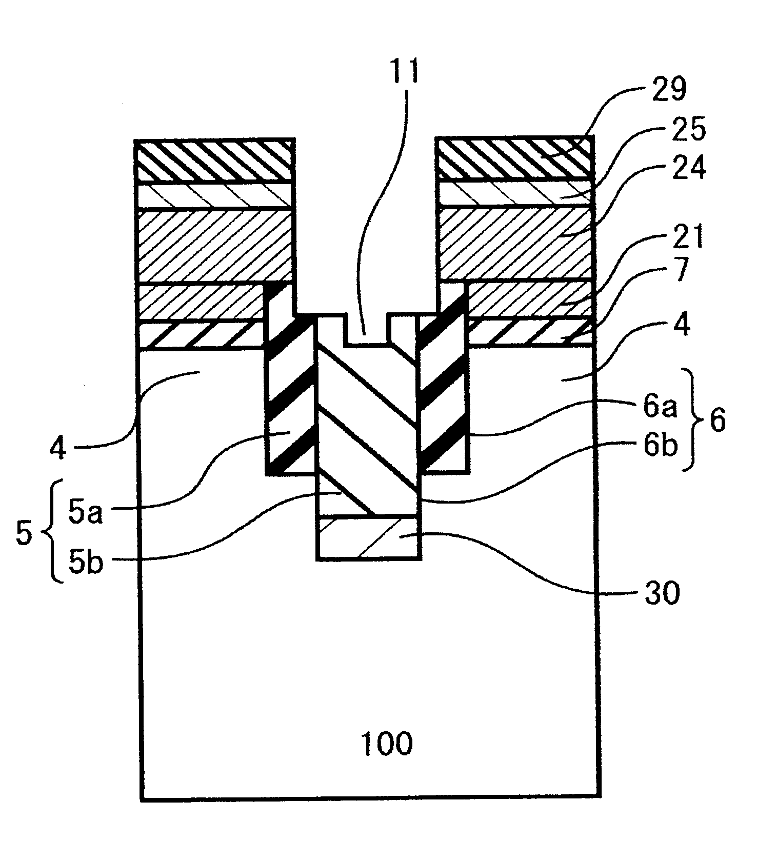
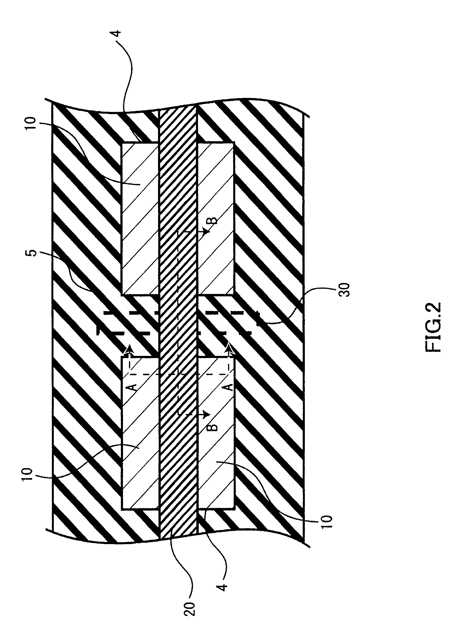
[0008]One aspect of this invention is to provide a semiconductor device comprises: a semiconductor substrate with a first impurity type; a plurality of active areas formed in the semiconductor substrate; an element isolation trench including a first trench part and a second trench part surrounding the plurality of active areas, the first trench part being extended from a surface of the semiconductor substrate to a depth direction, the second trench part being extended from the center of a bottom surface of the first trench part to the depth direction with a narrower width than the width of the first trench part in a width direction; an element isolation insulator film filled in the element isolation trench; a gate electrode formed on the plurality of active areas via a gate insulator film; a plurality of diffusion layers with a second impurity type formed in a surface of the plurality of active areas, the plurality of diffusion layers being located on each side of the element isolation trench and separated each other on each side of the gate electrode; and a channel stop region extended from the bottom surface of the second trench part to the depth direction in a predetermined depth with the first impurity type, the channel stop region having a higher impurity concentration than the impurity concentration of the semiconductor substrate.
[0009]Another aspect of this invention is to provide a method of manufacturing a semiconductor memory device comprises: forming a first trench part in a semiconductor substrate with a first impurity type; filling t

Problems solved by technology

However, a leakage current at a semiconductor substrate under the STI exists because of the high operation voltage.
However, with the method explained above, a residual photo resist may exist in the shallow trench due to an insufficient exposure of the photo resist at the bottom of the shallow trench caused by a large step between the surface of the semiconductor substrate and the bottom of the shallow trench.
The residual photo resist makes the ion implantation process unstable and a controllability of the impurity profile of the channel stop region is likely to become worse.

Method used


Image

  • Semiconductor device and manufacturing method thereof
  • Semiconductor device and manufacturing method thereof
  • Semiconductor device and manufacturing method thereof

Examples


Embodiment Construction

[0026]As a semiconductor memory device according to an embodiment of the invention, a NAND flash memory device is described with reference to the accompanying drawings. In the drawings to be referred to in the following description, the same or similar reference numerals designate the same or similar parts. The drawings are schematic, and the ratio between thickness and the planner dimension of each part, and the ratio among the thickness of layers differ from actual ones, for example.

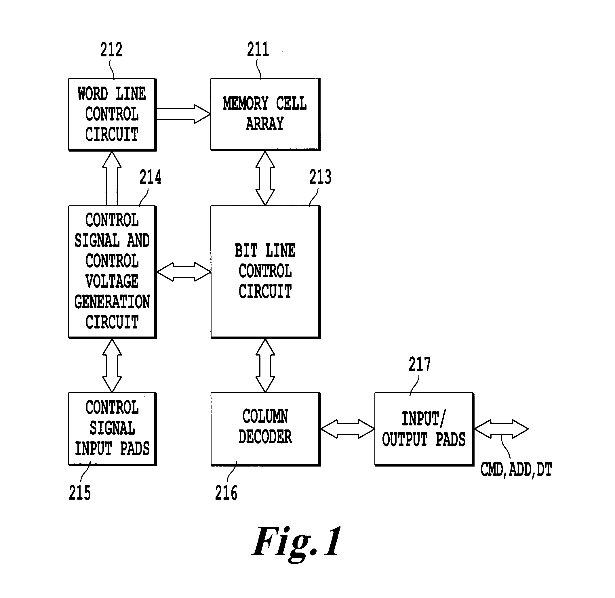
[0027]FIG. 1 is a block diagram of a NAND flash memory device according to the embodiment of the invention. As shown in FIG. 1, the NAND flash memory device includes memory cell arrays 211, a word line control circuit 212, a bit line control circuit 213, a control signal and control voltage generation circuit 214, control signal input pads 215, a column decoder 216, and data input / output pads 217.

[0028]The memory cell array 211 includes a plurality of blocks. The memory cell array 211 is coupled to the...


PUM


Abstract

This semiconductor device comprises a semiconductor substrate with a first impurity type; a plurality of active areas formed in the semiconductor substrate; an element isolation trench including a first trench part and a second trench part surrounding the plurality of active areas, the first trench part being extended from a surface of the semiconductor substrate to a depth direction, the second trench part being extended from the center of a bottom surface of the first trench part to the depth direction with a narrower width than the width of the first trench part in a width direction; an element isolation insulator film filled in the element isolation trench; a gate electrode formed on the plurality of active areas via a gate insulator film; a plurality of diffusion layers with a second impurity type formed in a surface of the plurality of active areas, the plurality of diffusion layers being located on each side of the element isolation trench and separated each other on each side of the gate electrode; and a channel stop region extended from the bottom surface of the second trench part to the depth direction in a predetermined depth with the first impurity type, the channel stop region having a higher impurity concentration than the impurity concentration of the semiconductor substrate.

Description

CROSS REFERENCE TO RELATED APPLICATIONS[0001]This application is based on and claims the benefit of priority from prior Japanese Patent Application No. 2008-277444, filed on Oct. 28, 2008, the entire contents of which are incorporated herein by reference.BACKGROUND OF THE INVENTION[0002]1. Field of the Invention[0003]The present invention relates to a semiconductor device and its fabrication process especially the device with high voltage transistors operated in a high voltage.[0004]2. Description of the Related Art[0005]In non-volatile semiconductor memory devices, such as flush memories, a high voltage of 20-30 V is necessary when data is programmed to memory cells. A plurality of high voltage transistors are employed, for example, in a word line driving circuit used for programming of data. The plurality of high voltage transistors are isolated each other by STI (Shallow Trench Isolation) including a shallow trench and an element isolation insulator film. However, a leakage curre...

Claims


Application Information

Patent Timeline
IPC IPC(8): H01L29/788H01L21/336
CPCH01L21/28114H01L21/76232H01L29/42376H01L27/11531H01L27/11526H10B41/40H10B41/42
Inventor AOI, TAKASHI
Owner KK TOSHIBA
Learn More