

Semiconductor device
- Summary
- Abstract
- Description
- Claims
- Application Information
AI Technical Summary
Benefits of technology
Problems solved by technology
Method used
Image

Examples
embodiment 1
Fifth Alteration of Embodiment 1
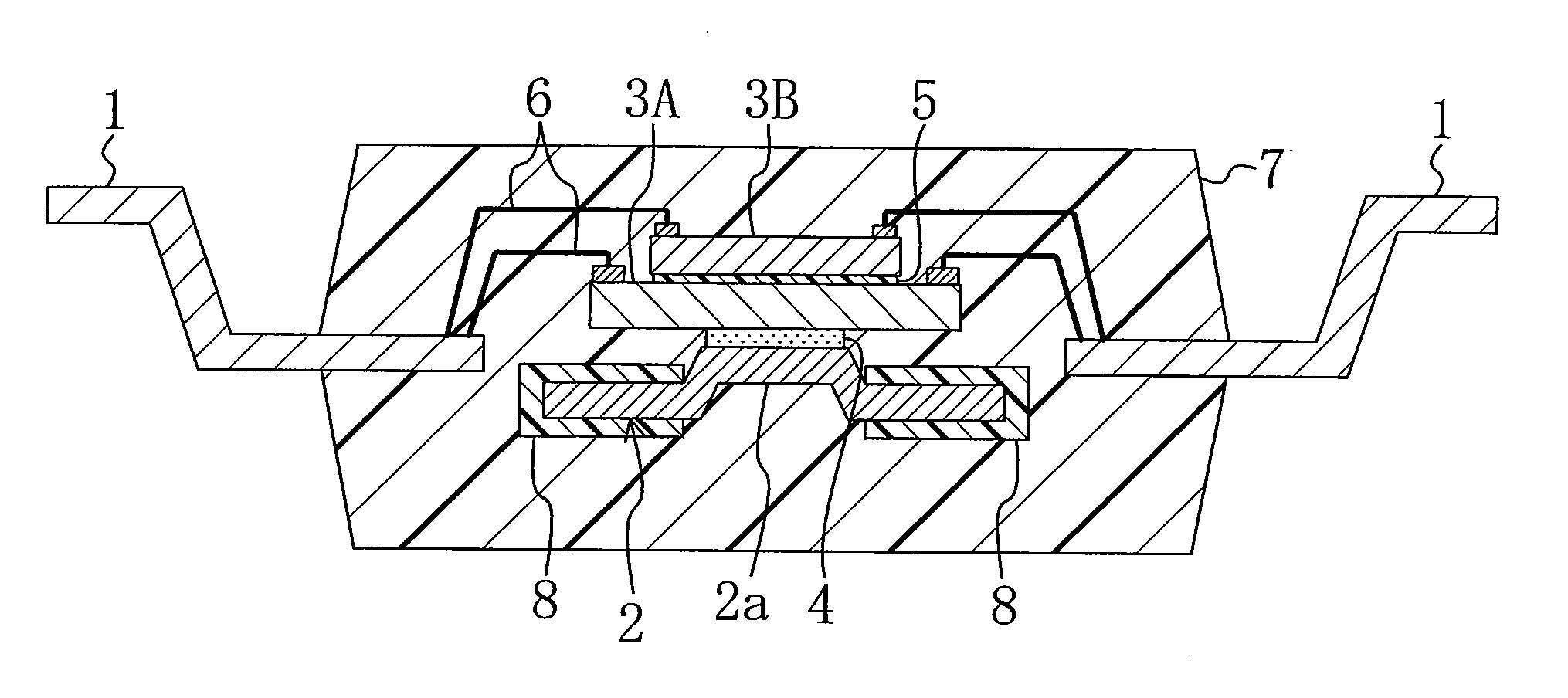
[0069]FIG. 4 shows a partial cross-sectional configuration of the peripheral portion of the die pad 2 and the buffer resin material 8 covering the peripheral portion.
[0070]In the fifth alteration, grains 9 made of an inorganic material or a metal high in thermal conductivity are added to or mixed in the buffer resin material 8. For the grains 9, silica, alumina, titania, aluminum, copper, silver or the like may be used. The added amount of the grains 9 to the buffer resin material 8 may be roughly in the range of 20% to 60%. Having such grains, the heat dissipation capability of the buffer resin material improves, and thus the reliability of the semiconductor device can be enhanced.
[0071]The fifth alternation is applicable to any of Embodiment 1 and the first to fourth alterations.
Embodiment 2
[0072]Example Embodiment 2 will be described with reference to the relevant drawings.
[0073]FIG. 5 diagrammatically shows a cross-sectional configuration of a ch...
embodiment 2
Alteration of Embodiment 2
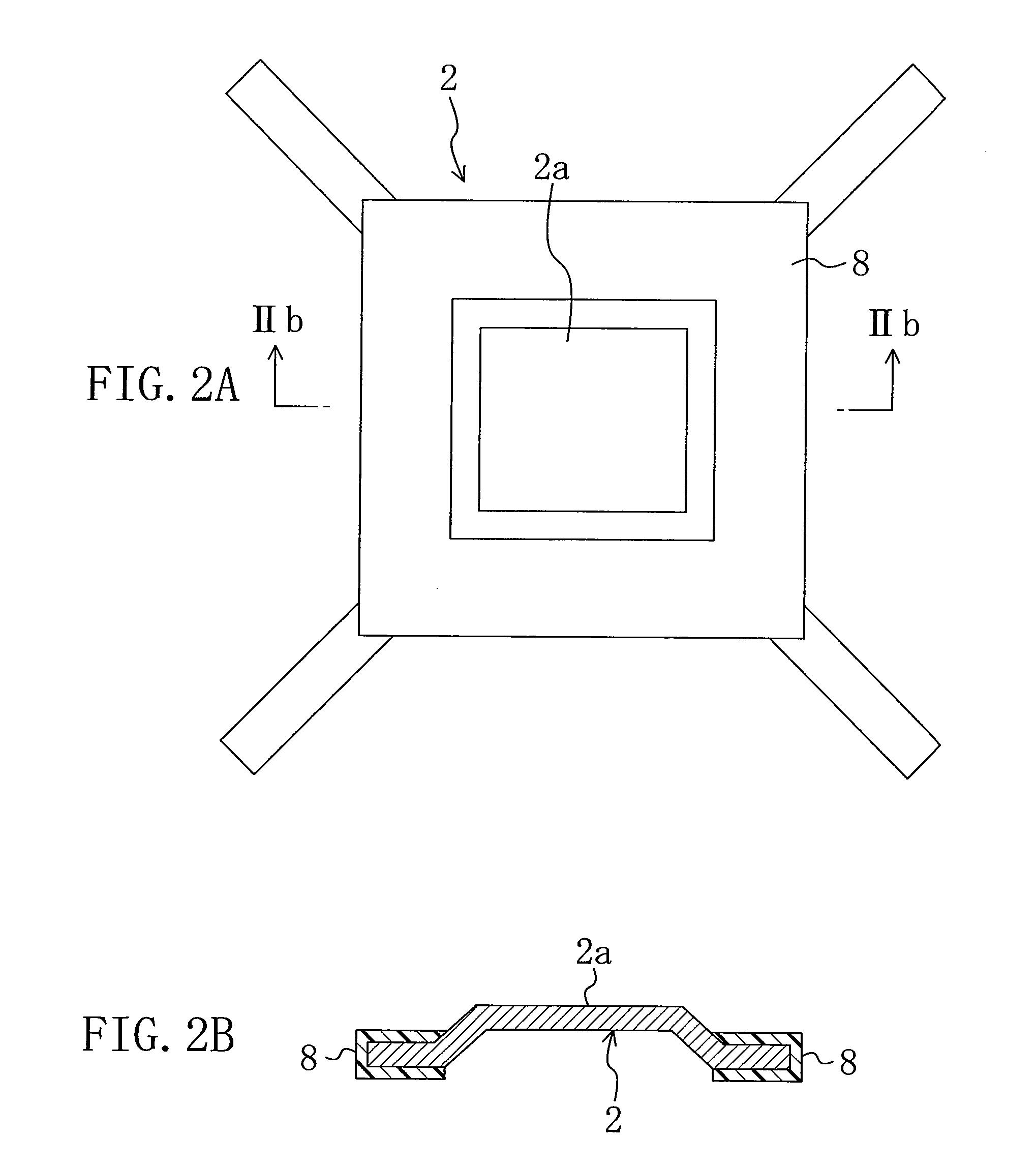
[0086]FIG. 7A shows a plan configuration of the die pad 2 having the upset portion 2a and the down-set portion 2b in an alteration of example Embodiment 2, and FIG. 3B shows a cross-sectional configuration taken along line VIIb-VIIb in FIG. 7A.
[0087]In general, when the sealing resin material 7 and the first and second semiconductor chips 3A and 3B are relatively thick, the thicknesses of the first and second semiconductor chips 3A and 3B and the sealing resin material 7 are dominant for the rigidity of the semiconductor device itself. In this case, warping does not occur with the stress at the contact portion between the top face of the upset portion 2a as the inner portion of the die pad 2 and the first semiconductor chip 3A attached together via the adhesive paste 4, which tends to expand or contract during temperature cycling testing and reflowing. Instead, interface fracture may occur with high probability.
[0088]In this alteration, therefore, the shape...
PUM
 Abstract
Description
Claims
Application Information