Contactless Interface

a contactless interface and interface technology, applied in the field of electronic interfaces, to achieve the effects of simple control loops, reduced size of decoupling capacitors, and faster acting regulators

Inactive Publication Date: 2010-04-29
INSIDE SECURE
View PDF10 Cites 8 Cited by
  • Summary
  • Abstract
  • Description
  • Claims
  • Application Information

AI Technical Summary

Benefits of technology

[0006]Power extracted from an antenna inductively coupled to an alternating magnetic field is regulated to provide voltage supplies. In some implementations, a first voltage supply (e.g., 3.8 volts) provides regulated voltage to analog circuits and a second, lower, voltage supply (e.g., 1.4 volts) provides regulated voltage to digital circuits. The first voltage supply can be regulated, using shunt regulation, by a first voltage regulator circuit. The first voltage supply can be output on a first voltage supply rail. The second voltage supply can be regulated, using series regulation, by a second voltage regulator circuit. The second voltage regulator circuit is supplied by the shunted current from the first voltage regulator circuit. Excess shunt current provided by the first voltage regulator circuit can be bypassed (e.g., bypassed to ground). The second voltage regulator circuit can use a timer circuit to control the amount of charge transferred to a second voltage supply rail. The timer circuit can compensate for the different currents from the first voltage regulator circuit. Bypassing excess shunt current obviates the need for the first voltage regulator control circuit to adapt to load changes on the second voltage supply rail.
[0007]Advantages of the disclosed contactless interface with switching regulator include, but are not limited, to a reduction in size of decoupling capacitors, faster acting regulators and simple control loops for the regulators that are easy to stabilize.

Problems solved by technology

These conventional smart cards suffer from processor noise (being seen by the card reader) which can cause various problems with reception by the reader of data from the smart card.

Method used


Image

  • Contactless Interface
  • Contactless Interface
  • Contactless Interface

Examples


example switching

Regulator Circuit

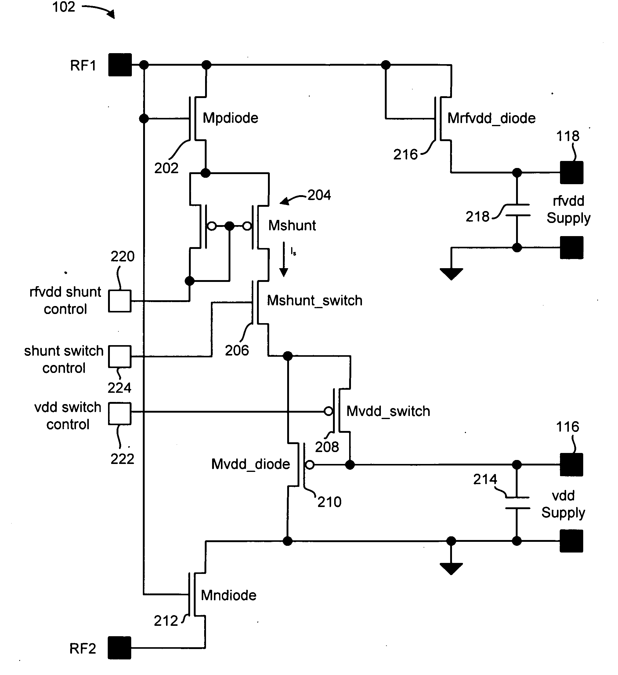
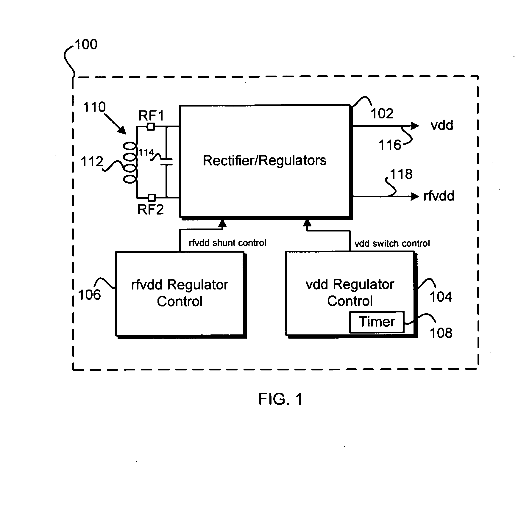
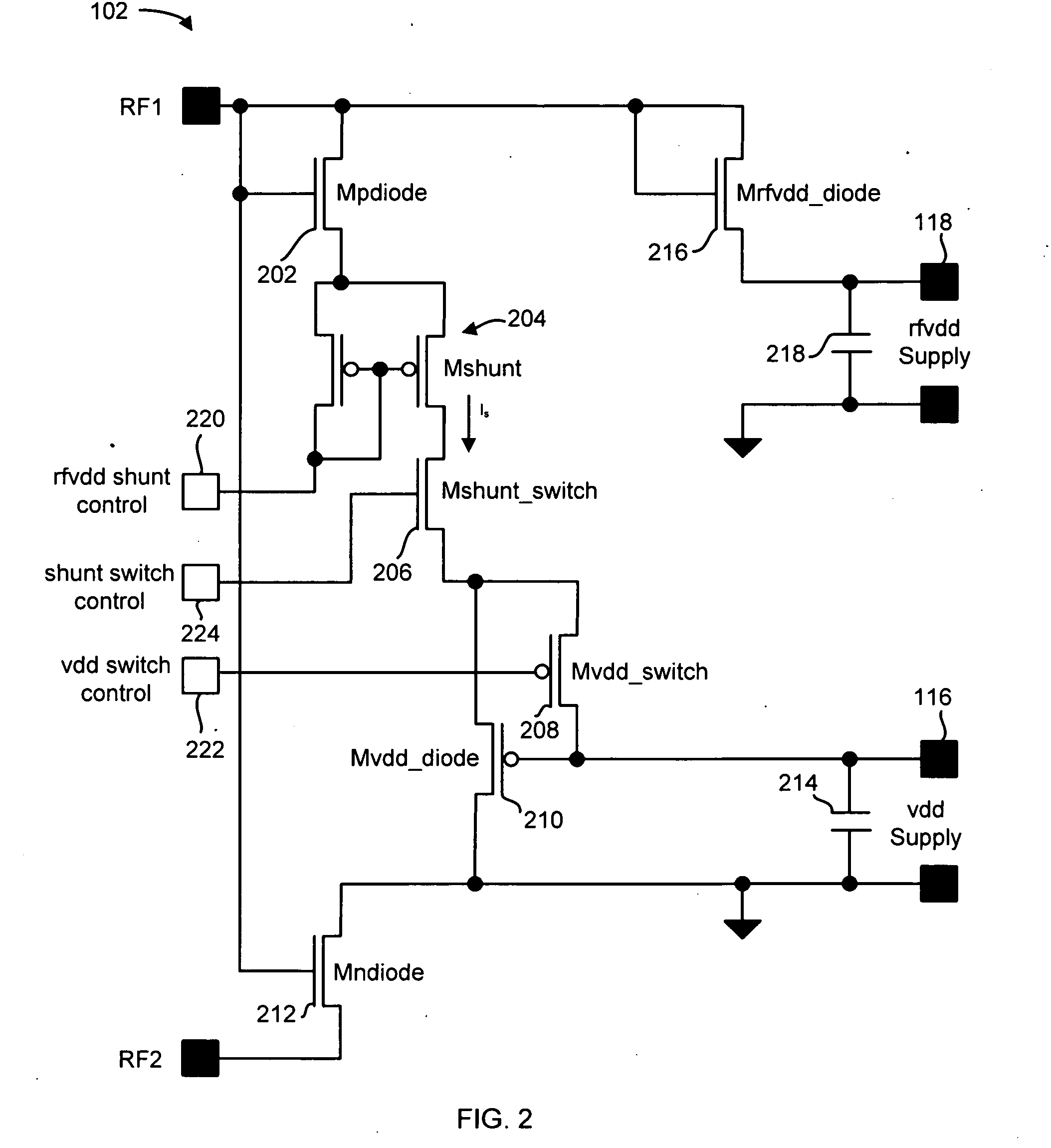
[0016]FIG. 2 is a simplified schematic diagram of example switching regulator circuit 102 of FIG. 1. The switching regulator circuit 102 is active when RF1 is at a higher potential then RF2. This is true for half of the carrier cycle. A second identical circuit can be used on the other half of the carrier cycle when RF2 is at a higher potential than RF1.

[0017]Rectification of the alternating current (“carrier signal”) output from resonant circuit 110 (e.g., antenna 112 and capacitor 114) is performed by devices 216 (Mrfvdd_diode), 202 (Mpdiode) and 212 (Mndiode). In some implementations, devices 216, 202, 212 are transistors (e.g., MOSFET) biased to operate as diodes, allowing current to flow in one direction through the devices. Devices 216, 202, 212 form a half bridge rectifier circuit. Device 212 couples RF2 to ground. Device 202 provides current to supply current mirror 204 (Mshunt) and vdd voltage supply rail 116. Device 216 provides current to supply circuits ...


PUM


Abstract

Power extracted from an antenna inductively coupled to an alternating magnetic field is regulated to provide voltage supplies. In some implementations, a first voltage supply (e.g., 3.8 volts) provides regulated voltage to analog circuits and a second, lower, voltage supply (e.g., 1.4 volts) provides regulated voltage to digital circuits. The first voltage supply is regulated, using shunt regulation, by a first voltage regulator circuit. The second voltage supply is regulated, using a series regulation, by a second voltage regulator circuit. The second voltage regulator circuit is supplied by the shunted current from the first voltage regulator. Excess shunt current provided by the first regulator circuit can be bypassed (e.g., bypassed to ground). The second voltage regulator circuit can use a timer circuit to control the amount of charge transferred to a second voltage supply rail. The timer circuit can compensate for different currents from the first voltage regulator circuit.

Description

TECHNICAL FIELD[0001]This subject matter relates generally to electronic interfaces, and more particularly to contactless interfaces for smart cards and other electronic devices.BACKGROUND[0002]A contactless smart card is commonly used for security access or payment systems. Contactless smart cards generally include an antenna, in the form of an inductor, coupled to an integrated circuit (IC). The IC commonly includes a capacitor which forms a resonant circuit with the antenna. A card reader presents an alternating magnetic field that excites the inductor / capacitor resonant circuit, which in turn energizes and powers the IC. The IC can then perform one or more functions, such as transmitting a card number through the antenna to the card reader.[0003]Some smart cards require supply voltages to power both digital (e.g., 1.4 volts) and analog circuits (e.g., 3.8 volts). The supply voltages are generated from the voltage across the capacitor in the resonant circuit. To ensure stable Dir...

Claims


Application Information

Patent Timeline
Patent Type & Authority Applications(United States)
IPC IPC(8): H02M7/00
CPCG06K19/0701G06K19/0723G06K19/0715
Inventor BATES, COLIN
Owner INSIDE SECURE
Why Eureka
Try Eureka