Nonvolatile memory apparatus

a memory apparatus and non-volatile technology, applied in the field of non-volatile memory apparatus, can solve the problems of data breakage, decrease in resistance value, etc., and achieve the effect of improving the reliability of a memory operation without reducing the speed of the write operation

Inactive Publication Date: 2010-04-29
PANASONIC SEMICON SOLUTIONS CO LTD
View PDF7 Cites 53 Cited by
  • Summary
  • Abstract
  • Description
  • Claims
  • Application Information

AI Technical Summary

Benefits of technology

[0041]The present invention has the above described configuration, and has an advantage that rel

Problems solved by technology

As a result, the resistance va

Method used


Image

  • Nonvolatile memory apparatus
  • Nonvolatile memory apparatus
  • Nonvolatile memory apparatus

Examples


embodiment 1

Apparatus Configuration

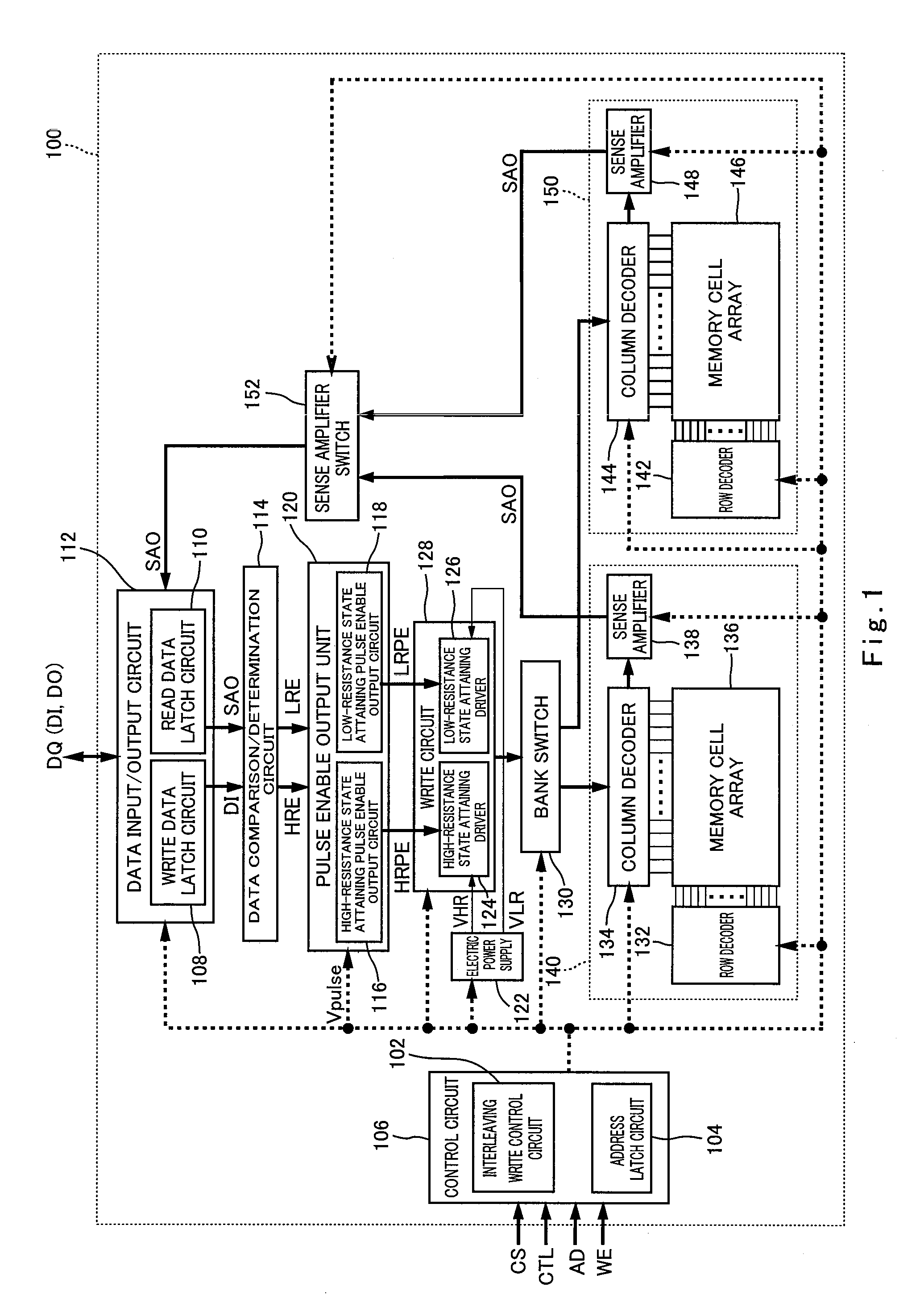
[0145]FIG. 1 is a block diagram showing an example of a schematic configuration of a nonvolatile memory apparatus according to Embodiment 1 of the present invention. Hereinafter, with reference to FIG. 1, a nonvolatile memory apparatus 100 of this embodiment will be described.

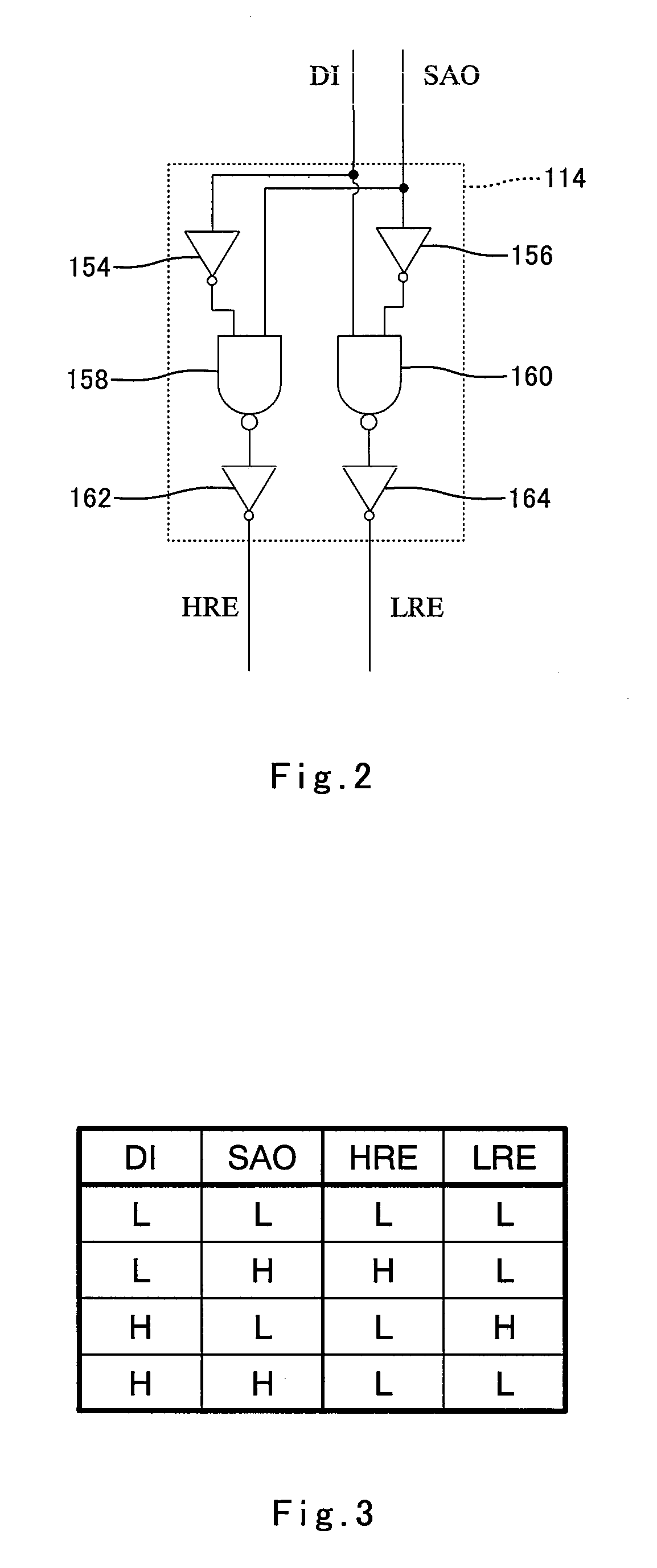
[0146]The nonvolatile memory apparatus 100 comprises a control circuit 106 including an interleaving write control circuit 102 and an address latch circuit 104, a data input / output circuit 112 including a write data latch circuit 108 and a read data latch circuit 110, a data comparison / determination circuit 114 (comparator / determiner portion), a pulse enable output unit 120 (pulse enable output portion) including a high-resistance state attaining pulse enable output circuit 116 and a low-resistance state attaining pulse enable output circuit 118, an electric power supply 122, a write circuit 128 (write portion) including a high-resistance state attaining driver 124 and a low-resistance st...

embodiment 2

[0211]The nonvolatile memory element 100 of Embodiment 1 is configured to perform the writing in which the data is read in advance, while a nonvolatile memory apparatus 200 of Embodiment 2 is configured to perform so-called “verify write” in addition to the writing in which the data is read in advance. As used herein, the term “verify write” means an operation in which after data is written to a memory element, the data held in the memory element is read for verification, the read data is compared to the write data, and writing is performed again if the read data and the write data do not match.

[0212]FIG. 13 is a block diagram showing a schematic configuration of the nonvolatile memory apparatus according to Embodiment 2 of the present invention. Hereinafter, with reference to FIG. 13, the nonvolatile memory apparatus 200 of this embodiment will be described. The nonvolatile memory apparatus 200 comprises a control circuit 206 including an interleaving write control circuit 202 and ...


PUM


Abstract

Provided are a plurality of memory cell arrays 136 and 146 each having a plurality of nonvolatile memory elements having a characteristic whose resistance value changes according to electric pulses applied, and control units (102, 104, 108, 110, 114, 128, 130, 152) configured to write data to a memory cell array and to read data from another memory cell array such that writing of the data and reading of the data occur concurrently in writing of the data to the plurality of memory cell arrays.

Description

TECHNICAL FIELD[0001]The present invention relates to a nonvolatile memory apparatus. More particularly, the present invention relates to a nonvolatile memory apparatus using a nonvolatile memory element whose resistance state changes according to electric signals applied.BACKGROUND ART[0002]Non-patent document 1 discloses a resistive random access memory apparatus as the conventional nonvolatile memory apparatus. In the resistive random access memory apparatus, a negative pulse (voltage: −2.0V, pulse width: 20 ns) is applied to change a memory cell using TiO2 / TiN as a resistance variable element to a low-resistance state (about 200Ω, “1” data), while a positive pulse (voltage: 2.2V, pulse width: 30 ns) is applied to change the memory cell to a high-resistance state (about 80 kΩ, “0” data).[0003]FIG. 16 is a view showing change in a resistance state in the case where positive and negative pulses are applied alternately in the resistive random access memory apparatus disclosed in the...

Claims


Application Information

Patent Timeline
IPC IPC(8): G11C11/00G11C8/00G11C7/00G11C7/10
CPCG11C11/56G11C11/5678G11C13/0004G11C13/003G11C13/0069G11C2216/22G11C2211/5623G11C2213/15G11C2213/74G11C2213/79G11C2013/0076
Inventor KAWAI, KENSHIMAKAWA, KAZUHIKO
Owner PANASONIC SEMICON SOLUTIONS CO LTD
Why Eureka
Try Eureka