
Resistance Variable Memory Device for Protecting Coupling Noise

a memory device and resistance variable technology, applied in the direction of information storage, static storage, digital storage, etc., can solve the problems of volatile memory that loses its stored data, and achieve the effect of preventing the effect of coupling nois

Active Publication Date: 2010-04-29
SAMSUNG ELECTRONICS CO LTD
View PDF3 Cites 8 Cited by
  • Summary
  • Abstract
  • Description
  • Claims
  • Application Information

AI Technical Summary

Benefits of technology

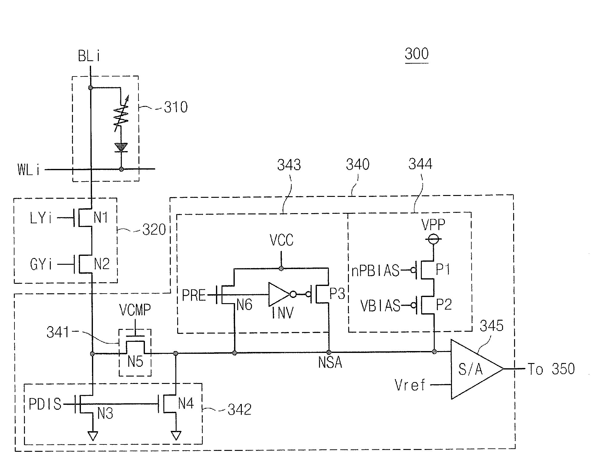
The present invention is about a resistance variable memory device that can prevent the effect of coupling noise. The device includes a memory cell, a precharge circuit, a bias circuit, and a control logic. The control logic provides a bias signal to the bias circuit at a precharge interval. The bias circuit then provides a bias voltage to the bit line to read the memory cell. The precharge circuit includes an NMOS transistor that is activated in response to a precharge signal. The precharge signal has a larger voltage level than the power supply voltage and a smaller voltage level than the bias voltage to prevent leakage current. The resistance variable memory device may also include a discharge circuit and a sense amplifier. The portable electronic system includes the resistance variable memory device and a central processing unit. The technical effects of the invention are to improve the accuracy and reliability of the resistance variable memory device and to reduce the impact of coupling noise on the device's performance.

Problems solved by technology

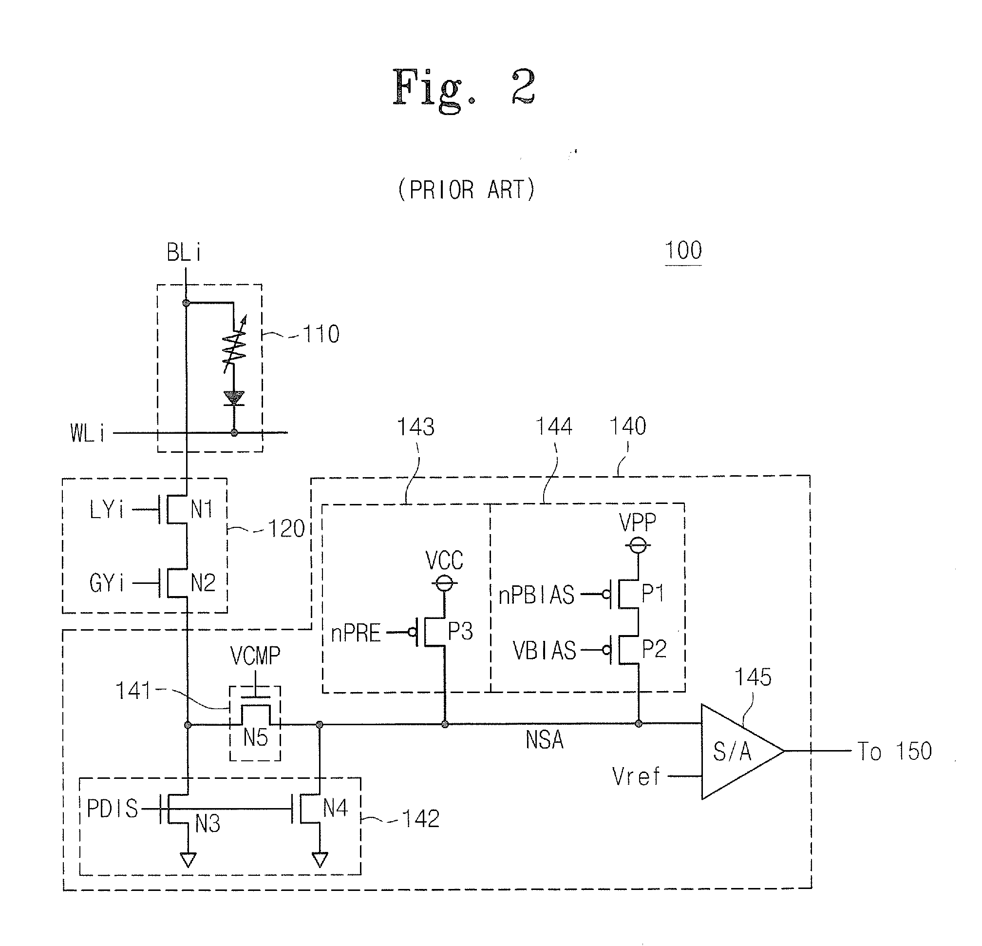
Meanwhile, the RAMs are a volatile memory that loses their stored data when the power supply is interrupted.

Method used


Image

  • Resistance Variable Memory Device for Protecting Coupling Noise
  • Resistance Variable Memory Device for Protecting Coupling Noise
  • Resistance Variable Memory Device for Protecting Coupling Noise

Examples


Embodiment Construction

[0026]Preferred embodiments of the present invention will be described below in more detail with reference to the accompanying drawings. The present invention may, however, be embodied in different forms and should not be constructed as limited to the embodiments set forth herein. Rather, these embodiments are provided so that this disclosure will be thorough and complete, and will fully convey the scope of the invention to those skilled in the art.

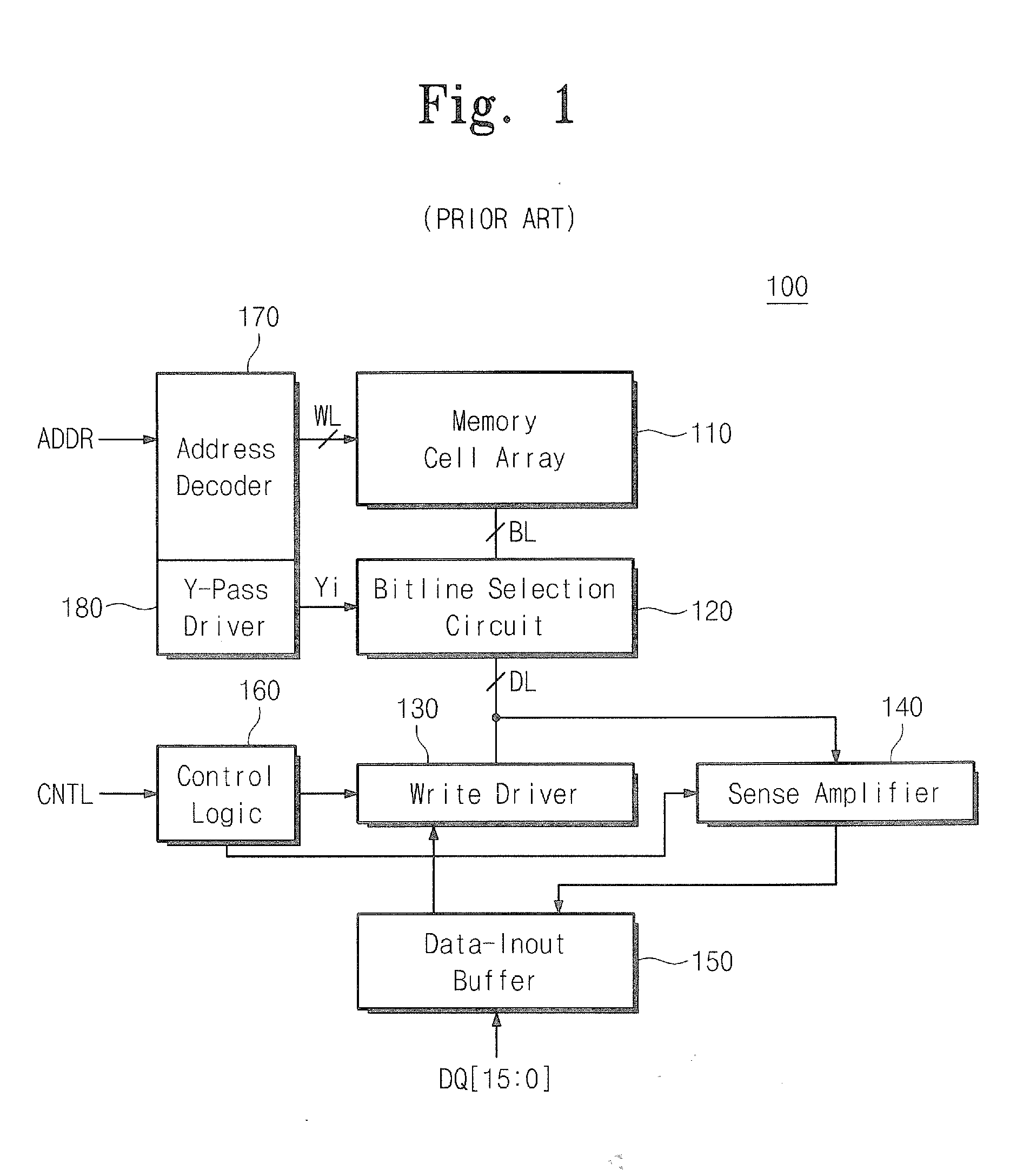
[0027]FIG. 1 is a block diagram of a general resistance variable memory device. Referring to FIG. 1, the resistance variable memory device 100 includes a memory cell array 110, a bit line selection circuit 120, a write driver 130, a sense amplifier 140, a data input and output buffer (data I / O buffer) 150, a control logic 160, an address decoder 170, and an Y-pass driver 180.

[0028]The memory cell array 110 may include a plurality of memory cells, and each memory cell may include a resistance variable memory element. Generally, the resista...


PUM


Abstract

The present invention relates to a resistance variable memory device, and more particularly, to a resistance variable memory device capable of preventing an effect of coupling noise. The resistance variable memory device includes: a memory cell connected to a bit line; a precharge circuit precharging the bit line in response to a precharge signal; a bias circuit providing a bias voltage to the bit line in response to,a bias signal; and a control logic controlling the precharge signal and the bias signal. The control logic provides the bias signal to the bias circuit at a precharge interval. Accordingly, the resistance variable memory device according to the present invention can prevent an effect coupling noise.

Description

REFERENCE TO PRIORITY APPLICATION[0001]This U.S. nonprovisional patent application claims priority to Korean Patent Application 10-2008-105399, filed Oct. 27, 2008, the contents of which are incorporated herein by reference.FIELD OF THE INVENTION[0002]The present invention relates to a resistance variable memory device, and more particularly, to a resistance variable memory device for preventing an effect of coupling noise.BACKGROUND OF THE INVENTION[0003]Semiconductor memory devices are storage devices that can store data and can output the stored data, if necessary. Generally, the semiconductor memory devices may be classified into Random Access Memories (RAMs) and Read-Only Memories (ROMs). The ROMs are a non-volatile memory that retains their stored data even when the power supply is interrupted. Examples of the ROMs include PROMs (Programmable ROMs), EPROMs (Erasable PROMs), EEPROMs (Electrically EPROMs), flash memories, and the like. The flash memories are classified into NOR-...

Claims


Application Information

Patent Timeline
Patent Type & Authority Applications(United States)
IPC IPC(8): G11C11/00G11C7/00
CPCG11C7/02G11C7/12G11C13/0004G11C2213/72G11C13/004G11C2013/0054G11C13/0026G11C7/06G11C13/0002
Inventor KIM, HOJUNGCHOI, JOON-YONG
Owner SAMSUNG ELECTRONICS CO LTD
Learn More