Method for making non-volatile memory

A non-volatile and manufacturing method technology, applied in the field of non-volatile memory manufacturing, can solve the problems of increased production cost of process steps, increased total thickness of dielectric layers, increased element resistance value, etc., so as to avoid the element resistance value. The effect of increasing, decreasing the total thickness, reducing the number of masks

Active Publication Date: 2008-06-25
POWERCHIP SEMICON MFG CORP +1
View PDF0 Cites 4 Cited by
  • Summary
  • Abstract
  • Description
  • Claims
  • Application Information

AI Technical Summary

Problems solved by technology

[0006] Since the above-mentioned source lines and contact plugs are formed, photolithography (photolithography), etching (etching) and chemical mechanical polishing (CMP) processes will be performed multiple times, so the process steps will be more complicated. complex
In addition, complex process steps and the use of a large number of masks will also lead to increased production costs
Furthermore, a multi-layer dielectric layer is formed in the process, and the thickness of the dielectric layer is increased in order to avoid the coupling effect (coupling effect) between the bit line and the source line, which also increases the total thickness of the dielectric layer, so that Voids are easily generated in the contact plug and cause an increase in the resistance value of the device

Method used


Image

  • Method for making non-volatile memory
  • Method for making non-volatile memory
  • Method for making non-volatile memory

Examples


Embodiment Construction

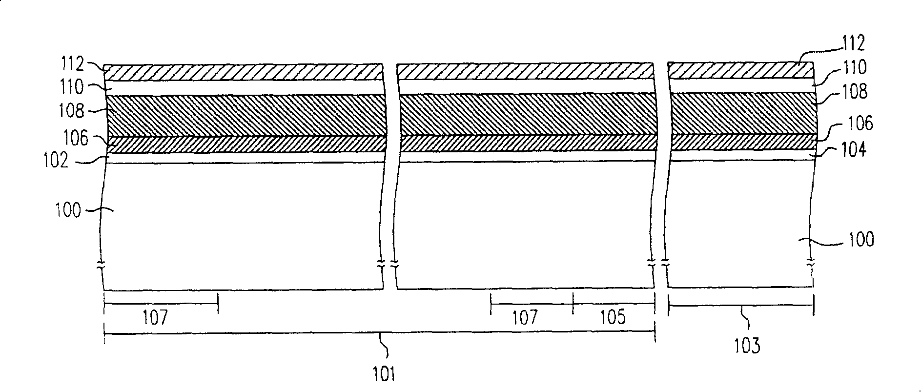
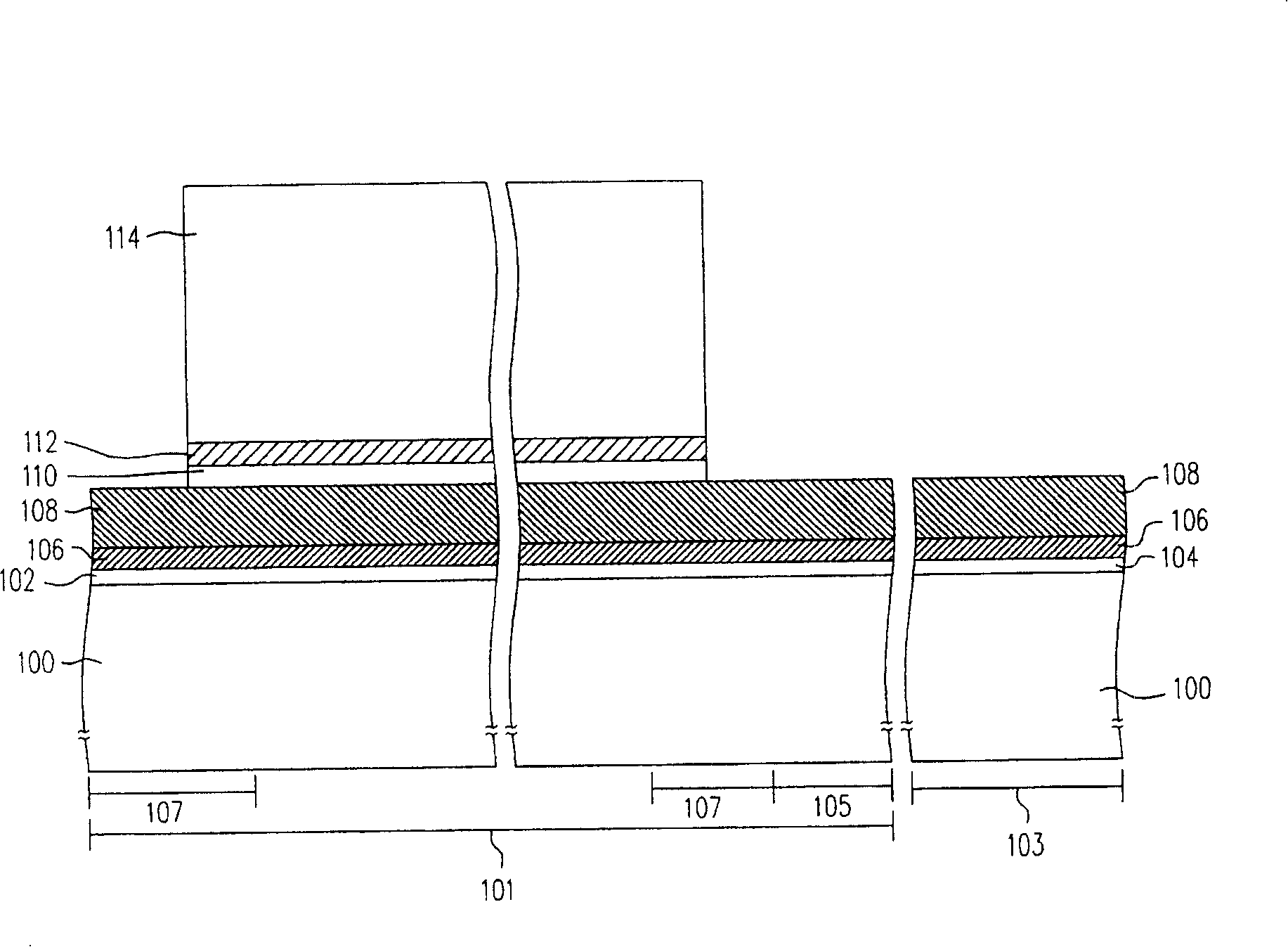
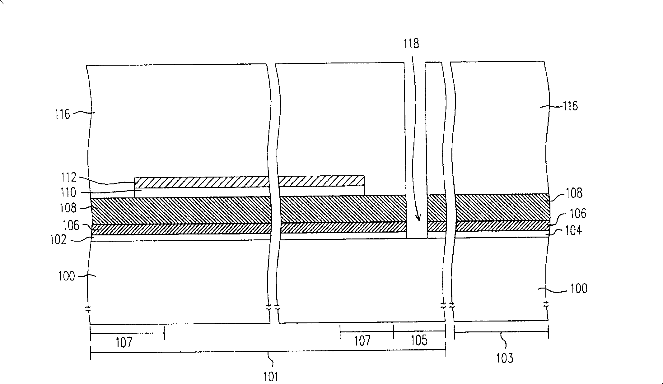
[0050] Figure 1A to Figure 1F It is a sectional view of the fabrication process of the non-volatile memory according to the embodiment of the present invention.

[0051] First, please refer to Figure 1A , a substrate 100 is provided, and the substrate 100 is, for example, a silicon substrate. The substrate 100 has a memory cell area 101 and a peripheral circuit area 103 . The memory cell region has a source line region 105 and a select gate region 107 .

[0052] Then, a tunnel dielectric layer 102 is formed on the substrate 100 in the memory cell area 101 , and a gate dielectric layer 104 is formed on the substrate 100 in the peripheral circuit area 103 . The materials of the tunneling dielectric layer 102 and the gate dielectric layer 104 are, for example, silicon oxide, and the methods for forming them are well known to those skilled in the art, and will not be repeated here. In addition, the thicknesses of the tunneling dielectric layer 102 and the gate dielectric laye...


PUM


Abstract

The invention relates to a fabricating method of a non-volatile memory. The method comprises the following steps: a substrate is provided firstly, and the substrate is provided with a source electrode line region. Secondly, a tunneling dielectric layer, a first conductor layer, an inter-gate dielectric layer and a second conductor layer are formed on the substrate in sequence. Thirdly, the second conductor layer and the inter-gate dielectric layer which are in the source electrode line region are removed, to ensure the first conductor layer to be exposed out. Fourthly, openings are formed in the first conductor layer which is in the source electrode line region and the tunneling dielectric layer. Fifthly, a third conductor layer is formed on the substrate, and the third conductor layers are filled into openings. Sixthly, the patterned process is performed, the third conductor layer , the second conductor layer, the inter-gate dielectric layer and the first conductor layer are all patterned, so as to form a plurality of stacked gate structures, and simultaneously a source electrode line is formed in the source electrode line region. Finally, doped regions are formed at the both sides of the stacked gate structures and in the substrate below the source electrode line.

Description

technical field [0001] The invention relates to a manufacturing method of a semiconductor element, and in particular to a manufacturing method of a nonvolatile memory. Background technique [0002] Non-volatile memory has the advantages of being able to store, read, and erase data multiple times, and the stored data will not disappear after power failure, so it has become widely used in personal computers and electronic devices. A type of non-volatile memory used. [0003] A typical non-volatile memory is generally designed with a stacked gate structure, including a floating gate and a control gate made of doped polysilicon. The floating gate is located between the control gate and the substrate, and is in a floating state, not connected to any circuit, while the control gate is connected to the word line (word line), and also includes a tunnel oxide layer A tunneling oxide layer and an inter-gate dielectric layer are located between the substrate and the floating gate and...

Claims


Application Information

Patent Timeline
Patent Type & Authority Applications(China)
IPC IPC(8): H01L21/8247H01L21/768
Inventor 简财源王子嵩
Owner POWERCHIP SEMICON MFG CORP
Why Eureka
Try Eureka