Operational amplifier

a technology of operation amplifier and phase margin, which is applied in the direction of rf amplifier, gated amplifier, amplifier with semiconductor device/discharge tube, etc., can solve the problems of increased oscillation possibility, increased oscillation possibility, and difficulty in transmitting high-speed signals, so as to increase the slew rate and increase the capacitance of capacitors. , increase the phase margin

Inactive Publication Date: 2010-05-06
RENESAS ELECTRONICS CORP
View PDF3 Cites 6 Cited by
  • Summary
  • Abstract
  • Description
  • Claims
  • Application Information

AI Technical Summary

Benefits of technology

[0012]In the operational amplifier according to the exemplary aspect of an embodiment of the present invention, the charge and discharge current of the capacitor connected between the input node and the output node of the output stage amplifier is controlled by the charge and discharge control circuit. Specifically, even when the output voltage of the operational amplifier makes transition, the charge and discharge current of the capacitor is controlled by the charge and discharge control circuit. Thus, in the operational amplifier according to the exemplary aspect of an embodiment of the present invention, it is possible to ignore the capacitance of the capacitor with respect to the slew rate. Accordingly, in the operational amplifier according to the exemplary aspect of an embodiment of the present invention, it is possible to increase the slew rate as well as increasing the phase margin by increasing the capacitance of the capacitor. Further, there is no need to increase the output current of the input stage amplifier in order to improve the slew rate.
[0013]According to the exemplary aspect of an embodiment of the present invention, it is possible to provide an operational amplifier capable of improving the slew rate while maintaining a sufficient phase margin and lowering the current consumption.

Problems solved by technology

In the operational amplifier, defects such as oscillation possibly occur if the phase margin of the operational amplifier is small.
However, if the capacitance of the capacitor decreases, the phase margin of the operational amplifier 100 decreases, which causes the possibility of oscillation to increase.
Therefore, the operational amplifier 100 has a problem that it is difficult to transmit a high-speed signal while maintaining a sufficient phase margin and lowering the current consumption of the amplifier.

Method used


Image

  • Operational amplifier
  • Operational amplifier
  • Operational amplifier

Examples


first exemplary embodiment

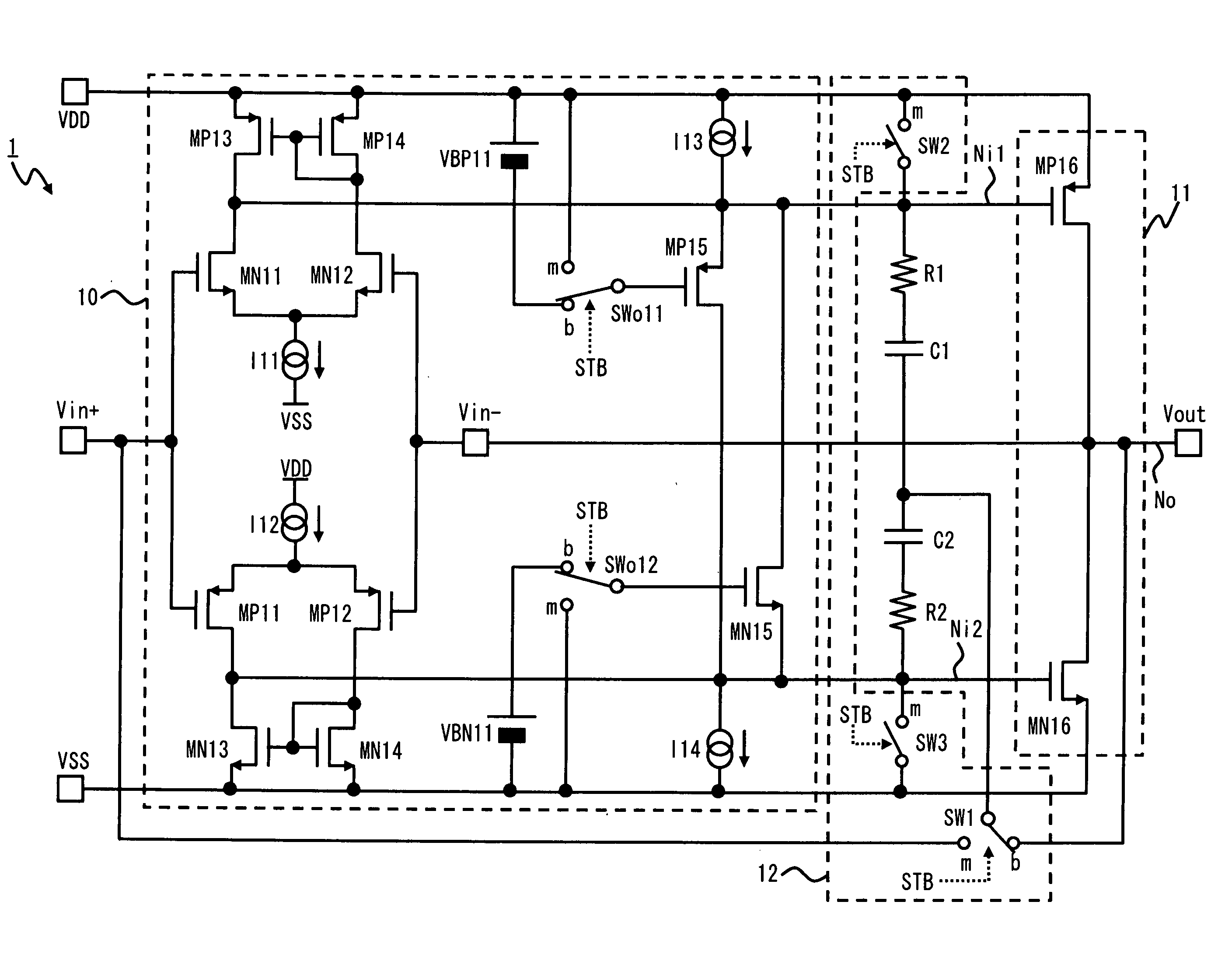
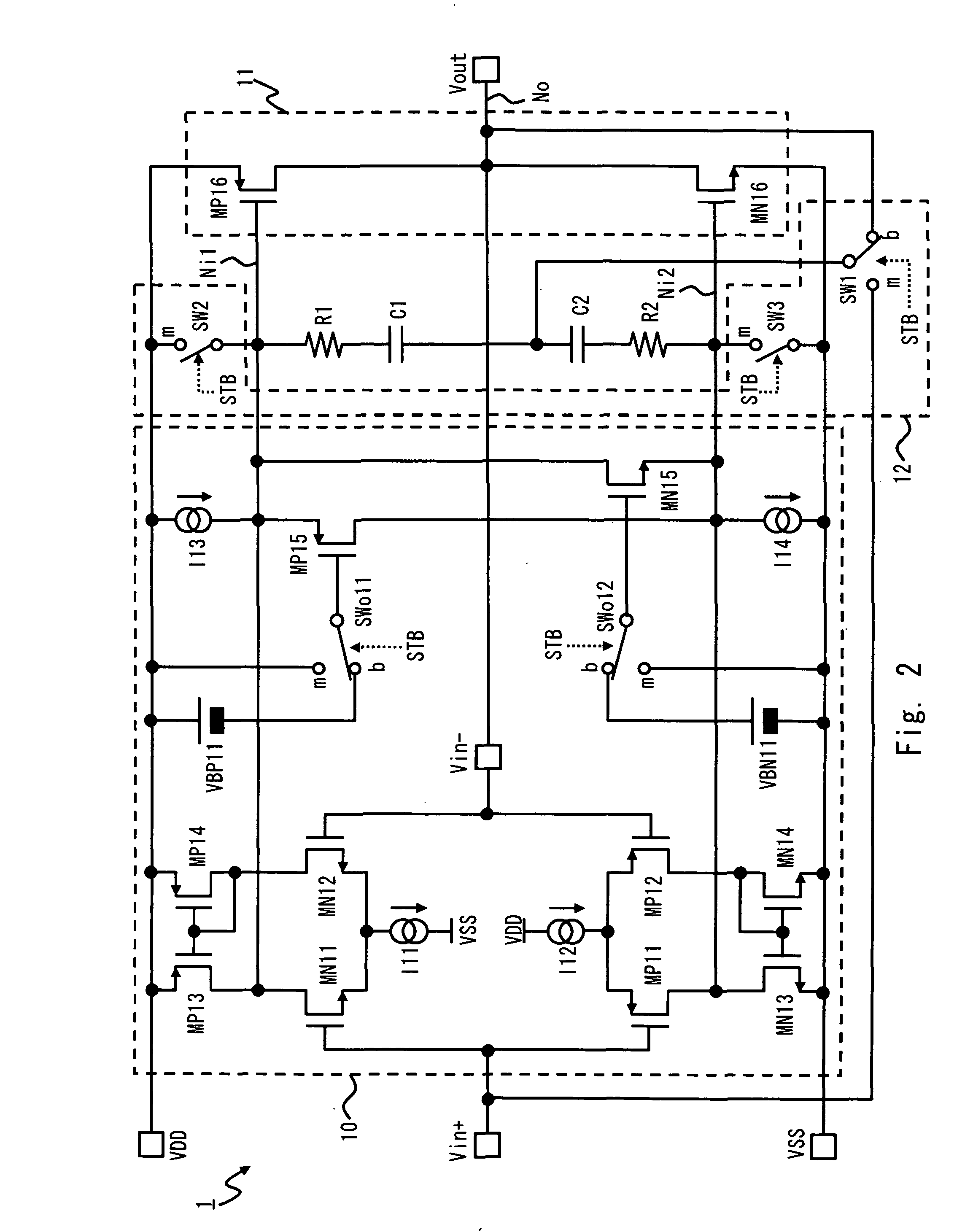
[0031]Exemplary embodiments of the present invention are described hereinafter with reference to the drawings. FIG. 1 shows a block diagram of an operational amplifier 1 according to a first exemplary embodiment of the present invention. Referring to FIG. 1, the operational amplifier 1 includes an input stage amplifier 10, an output stage amplifier 11, a charge and discharge control circuit 12, a first capacitor (e.g. a capacitor C1), and a second capacitor (e.g. a capacitor C2). The input stage amplifier 10 has a non-inverting input terminal and an inverting input terminal. The input stage amplifier 10 and the output stage amplifier 11 are connected in series, and the output node of the output stage amplifier 11 is connected to the inverting input terminal of the input stage amplifier 10. The operational amplifier 1 thereby operates as a buffer.

[0032]The input stage amplifier 10 outputs a first signal and a second signal that are in-phase with each other based on a signal input to ...

second exemplary embodiment

[0071]FIG. 8 is a block diagram showing an operational amplifier 2 according to a second exemplary embodiment of the present invention. Referring to FIG. 8, the operational amplifier 2 is configured by altering the connection of the switch SW1 in the operational amplifier 1 and adding a voltage source VG1 as the first power supply. In the switch SW1 of the operational amplifier 2, the terminals of the capacitors C1 and C2 on the output node side are connected to the common terminal c, the output node No is connected to the break terminal b, and the positive electrode of the voltage source VG1 is connected to the make terminal m. The negative electrode of the voltage source VG1 is connected to the negative power supply VSS.

[0072]Thus, in the operational amplifier 2, it is possible to arbitrarily set the voltages to be applied to the terminals of the capacitors C1 and C2 on the output node side during the charge recovery period according to the setting of the voltage value to be gener...

third exemplary embodiment

[0073]FIG. 9 is a block diagram showing an operational amplifier 3 according to a third exemplary embodiment of the present invention. Referring to FIG. 9, the operational amplifier 3 is configured by replacing the second switch (the switch SW2 and the switch SW3) in the operational amplifier 1 with transfer type switches and adding voltage sources VG2 and VG3 as the second power supply. In the switch SW2 of the operational amplifier 3, the terminal of the capacitor C1 on the input node side is connected to the common terminal c, the input node Ni1 is connected to the break terminal b, and the negative electrode of the voltage source VG2 is connected to the make terminal m. The positive electrode of the voltage source VG2 is connected to the positive power supply VDD. In the switch SW3 of the operational amplifier 3, the terminal of the capacitor C2 on the input node side is connected to the common terminal c, the input node Ni2 is connected to the break terminal b, and the positive...


PUM


Abstract

An operational amplifier includes an input stage amplifier that receives an input signal, an output stage amplifier that amplifies a signal output from the input stage amplifier and outputs the signal, a capacitor that is connected between an input node and an output node of the output stage amplifier, and a charge and discharge control circuit that controls a charge and discharge current of the capacitor.

Description

CROSS-REFERENCE TO RELATED APPLICATIONS[0001]The present invention is a Continuation-in-Part (CIP) application of commonly-assigned, co-pending, U.S. patent application Serial No. 12 / 457,554 filed Jun. 15, 2009 which is hereby incorporated by reference in their entirety.BACKGROUND[0002]1. Field of the Invention[0003]The present invention relates to an operational amplifier and, particularly, to an operational amplifier that includes a capacitor between an input node and an output node of an output stage amplifier.[0004]2. Description of Related Art[0005]In semiconductor devices, operational amplifiers are widely used to amplify signals to be handled. An example of operational amplifiers is disclosed in Japanese Unexamined Application Patent Publication No. H6-326529 (U.S. Pat. No. 5,311,145). An operational amplifier includes an input stage amplifier and an output stage amplifier. The input stage amplifier converts an input signal according to the input structure of the output stage...

Claims


Application Information

Patent Timeline
Patent Type & Authority Applications(United States)
IPC IPC(8): H03F3/45
CPCH03F3/4521H03F3/45475H03F3/72H03F2200/411H03F2200/451H03F2203/45138H03F2203/45248H03F2203/45512H03F2203/45536H03F2203/45648H03F2203/45726H03F2203/7227
Inventor NISHIMURA, KOUICHIHORI, YOSHIHIKO
Owner RENESAS ELECTRONICS CORP
Why Eureka
Try Eureka