Semiconductor device having resistors with a biased substrate voltage

a technology of resistor elements and semiconductor devices, which is applied in the direction of resistor details, positive-feedback circuit arrangements, transistors, etc., can solve the problems of unstable characteristic of the circuit formed of resistor elements, distortion components that are significant problems, and distortion that occurs in the output signal of the amplifier. to achieve the effect of inhibiting signal distortion

Inactive Publication Date: 2010-05-06
RENESAS ELECTRONICS CORP
View PDF12 Cites 30 Cited by
  • Summary
  • Abstract
  • Description
  • Claims
  • Application Information

AI Technical Summary

Benefits of technology

[0011]In the series-coupled resistor elements, the voltages between the substrate regions and the resistor elements have the opposite polarities. Accordingly, the substrate voltage dependences of the respective resistance values of the series-coupled resistor elements are inhibited or cancelled therebetween and hence, the substrate voltage dependence of the resistance value of the entire seque

Problems solved by technology

In particular, when the resistor element is used in an op-amp, the amplification factor thereof varies according to the substrate voltage dependence of the resistance value thereof, and the waveform of an output signal therefrom deviates from the waveform of an ideal response characteristic so that distortion occurs in an output signal from the amplifier.
In particular, in a recently practiced application in which high accuracy is required such as image processing or audio processing, the distortion component presents a si

Method used


Image

  • Semiconductor device having resistors with a biased substrate voltage
  • Semiconductor device having resistors with a biased substrate voltage
  • Semiconductor device having resistors with a biased substrate voltage

Examples


embodiment 1

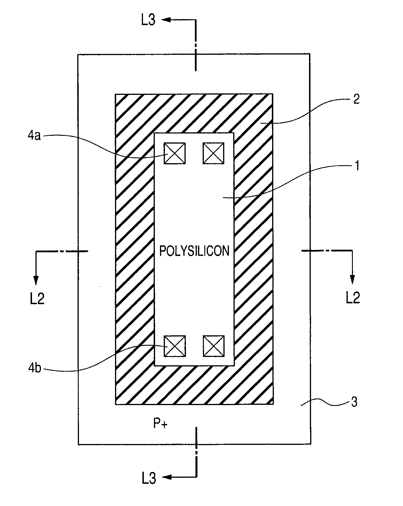
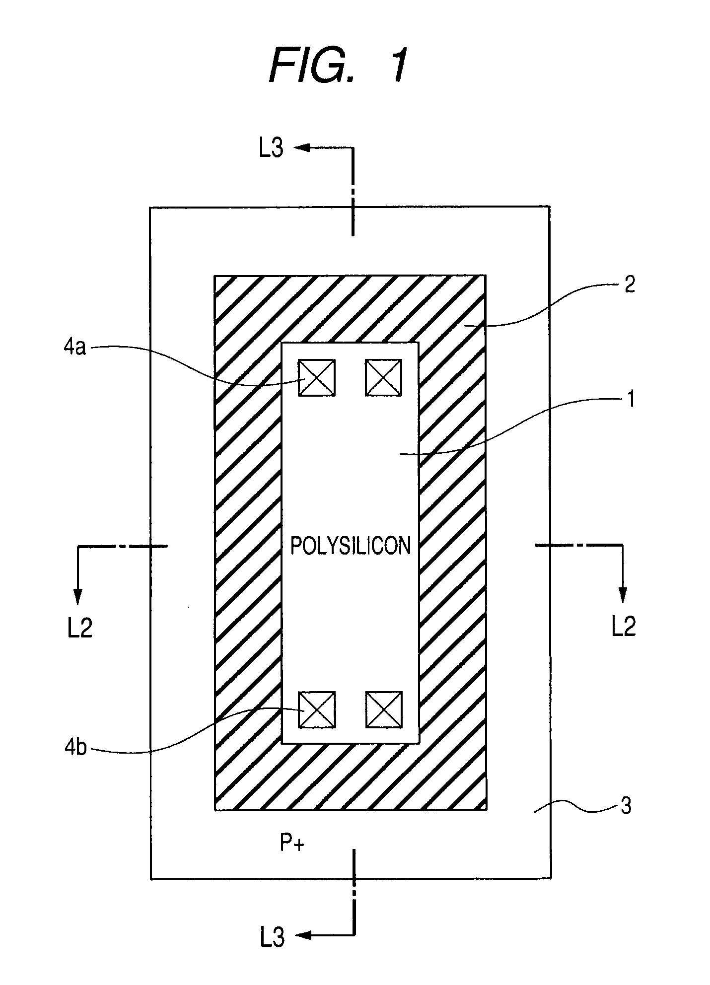
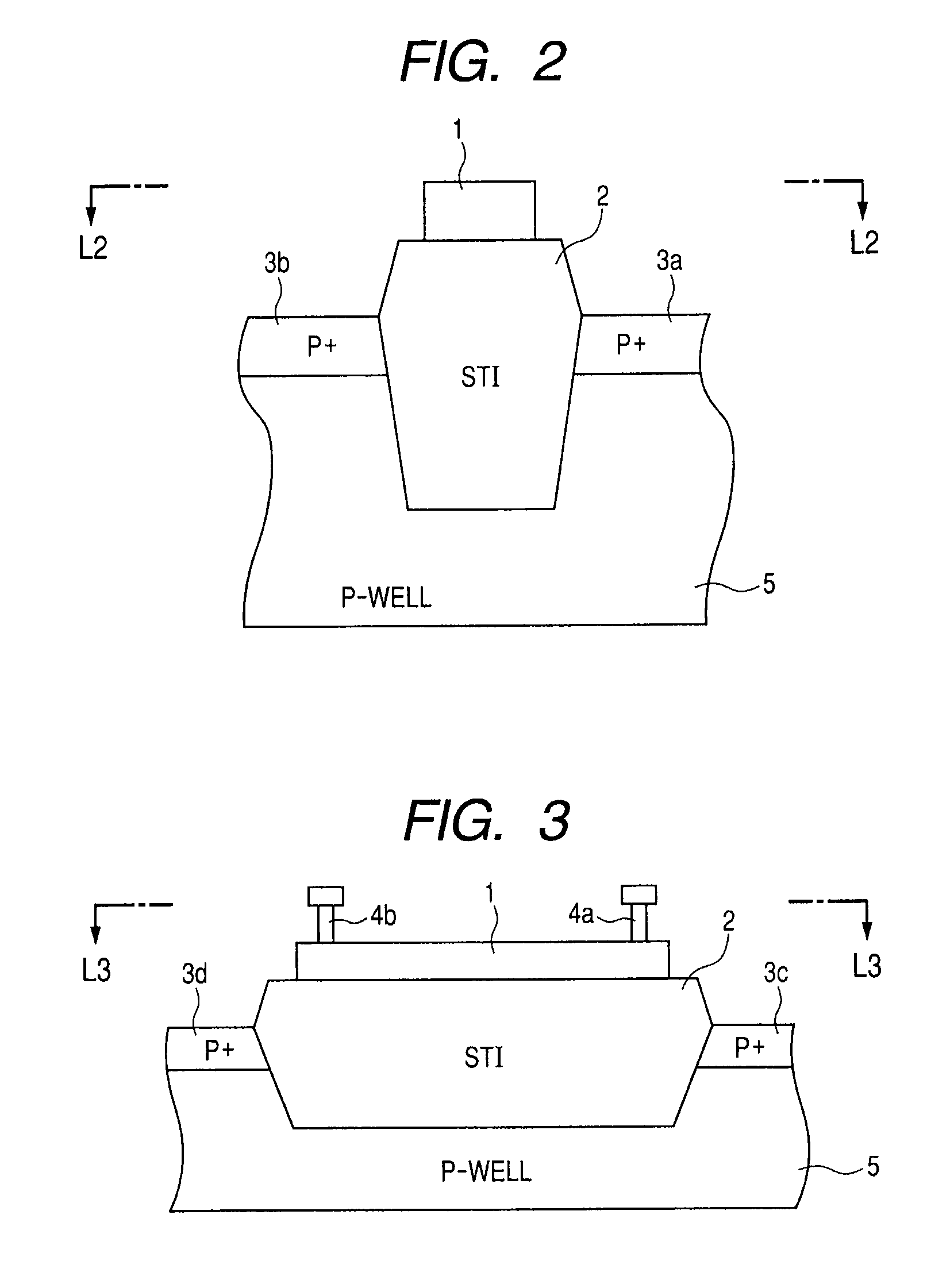
[0060]FIG. 1 is a view schematically showing a two-dimensional layout of a resistor element used in the present invention. In FIG. 1, a polysilicon resistive element 1 having a rectangular shape, and forming the resistor element is disposed over an isolation film 2. The isolation film 2 is, e.g., a shallow trench isolation (STI) film. In a surface of a substrate region (not shown in FIG. 1) around the isolation film 2, there is provided a high-concentration impurity region 3. An example of the high-concentration impurity region 3 is a high-concentration P-type impurity layer in which a P-type impurity has been implanted at a high concentration. Through the high-concentration impurity region 3, a substrate bias voltage is supplied to a well region (substrate region) formed under the high-concentration impurity region 3 (substrate bias voltage for supplying a voltage to a substrate will be described later in detail). The P-type impurity region 3 is used because the polysilicon of the ...

embodiment 2

[0087]FIG. 10 is a view showing the coupling of resistor elements according to Embodiment 2 of the present invention. In FIG. 10, the resistor elements R1 and R2 are coupled in series between the nodes A and C. The coupling node B between the resistor elements R1 and R2 is electrically coupled to the respective substrate regions of the resistor elements R1 and R2. Each of the resistor elements R1 and R2 has the equal resistance value R.

[0088]In a form of substrate voltage supply to the resistor elements R1 and R2 shown in FIG. 10, the average potentials Vx(AB) and Vx(BC) from the respective substrate regions of the resistor elements R1 and R2 are given by the following respective expressions.

[0089]Average Potential from Substrate between nodes A and B: Vx(AB)=(Va+Vb) / 2−Vb=−(−Va+C) / 4. Average Potential from Substrate between nodes B and C: Vx(BC)=(Vb+Vc) / −Vb=(−Va+Vc) / 4. Therefore, in the coupling form of the substrate regions of the resistor elements shown in FIG. 10, the average pot...

embodiment 3

[0098]FIG. 14 is a view schematically showing a two-dimensional layout of resistor elements according to Embodiment 3 of the present invention. In FIG. 14, the resistor elements R1 and R2 are coupled in series between the nodes A and B, and the potential at the coupling node B between the resistor elements R1 and R2 is transmitted to a P-well 45 through a high-concentration impurity region 42, in the same manner as in Embodiment 2. The two-dimensional layout of the resistor elements R1 and R2 is the same as the two-dimensional layout shown in FIG. 12 except that the coupling wires 26A and 26C extend in the longitudinal direction of the drawing. In FIG. 14, the portions of the resistor elements R1 and R2 corresponding to those in the two-dimensional layout shown in FIG. 12 are denoted by the same reference numerals, and a detailed description thereof is omitted.

[0099]In the two-dimensional layout shown in FIG. 14, at locations outside the isolation film 22A, isolation films 42A and 4...


PUM


Abstract

To eliminate the substrate voltage dependences of the respective resistance values of resistor elements, in the resistor elements coupled in series to each other over respective substrate regions, the ends of the resistor elements are coupled to the corresponding substrate regions by respective bias wires such that respective average potentials between the substrate regions of the resistor elements and the corresponding resistor elements have opposite polarities, and equal magnitudes.

Description

CROSS-REFERENCE TO RELATED APPLICATIONS[0001]The disclosure of Japanese Patent Application No. 2008-281160 filed on Oct. 31, 2008 including the specification, drawings and abstract is incorporated herein by reference in its entirety.BACKGROUND OF THE INVENTION[0002]The present invention relates to semiconductor devices, and particularly to a semiconductor device using resistor elements such as polysilicon resistors. More particularly, the present invention relates to a configuration which inhibits the substrate voltage dependences of resistor elements such as polysilicon resistors.[0003]In a semiconductor circuit device, resistor elements are used in various portions thereof. To implement a desired operation characteristic of a circuit, a resistor element is required to precisely retain the resistance value thereof. Typically, when a diffused resistor using the resistance of an impurity layer (diffusion layer) is used as a resistor element, the size of a depletion layer differs acco...

Claims


Application Information

Patent Timeline
IPC IPC(8): H03F3/45H01C1/012H03F3/04
CPCH01L27/0802H01L28/20H03F2203/45602H03F2203/45528H03F2203/45594H03F3/45475
Inventor KAMAKURA, MASAOMIKUMAMOTO, TOSHIOOKUDA, TAKASHI
Owner RENESAS ELECTRONICS CORP
Why Eureka
Try Eureka