Method for forming fine contact hole pattern of semiconductor device

a technology of contact hole pattern and semiconductor device, which is applied in the direction of photomechanical equipment, instruments, originals for photomechanical treatment, etc., can solve the problems of difficult to obtain a fine pattern reduced with a uniform size, difficult to form a contact hole pattern of less than 50 nm,

Active Publication Date: 2010-05-06
SK HYNIX INC
View PDF4 Cites 24 Cited by
  • Summary
  • Abstract
  • Description
  • Claims
  • Application Information

AI Technical Summary

Benefits of technology

[0010]In another embodiment, the present invention relates to a method for forming a fine contact hole pattern of a semiconductor device that comprises performing a two-step etching process using two kinds of exposure masks, thereby obtaining a fine pattern that has a reduced minimum pattern pitch.
[0014]The mask pattern that has a different etching selectivity ratio from that of the insulating film and the underlying layer is a material that can be used as a mask in the etching process performed on the underlying layer. For example, the mask film includes an amorphous carbon layer. The insulating film includes an oxide film, a nitride film and an oxide nitride film that can be easily etched in the etching process using the photoresist pattern as an etching mask.
[0022]In the aforementioned method, it is possible to obtain a contact hole having a fine pattern pitch which is smaller than the minimum pattern pitch obtained by the current exposer through the two-step etching process.

Problems solved by technology

It is difficult to form a contact hole pattern of less than 50 nm using a single ArF exposure process that has a numerical aperture (NA) of less than 1.0 even though an immersion lithography process is performed.
Also, since the amount of flowing photoresist is different depending on pattern density, it is difficult to obtain a fine pattern reduced with a uniform size.
In other words, it is difficult to obtain a contact hole pattern reduced with a uniform size over a wafer.
As a result, it is impossible to obtain a stable process margin for a subsequent process, thereby degrading yield and reliability of the device.

Method used


Image

  • Method for forming fine contact hole pattern of semiconductor device
  • Method for forming fine contact hole pattern of semiconductor device
  • Method for forming fine contact hole pattern of semiconductor device

Examples


Embodiment Construction

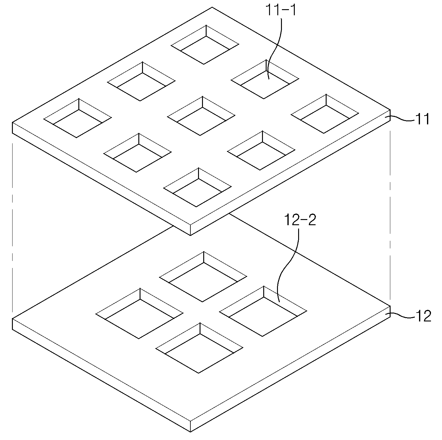
[0026]Referring to FIG. 2, a first exposure mask (11) including a plurality of rectangular light transmitting regions (11-1) each having a given (minimum) pitch and a second exposure mask (12) including a plurality of rectangular light transmitting regions (12-1) each having a given (minimum) pitch are provided.

[0027]FIGS. 3a to 3e are diagrams illustrating a method for forming a pattern of a semiconductor device according to an embodiment of the present invention.

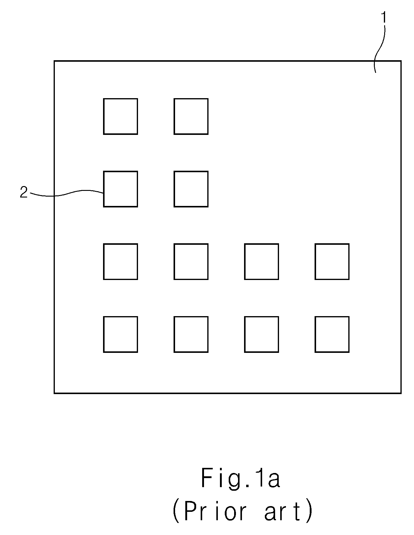
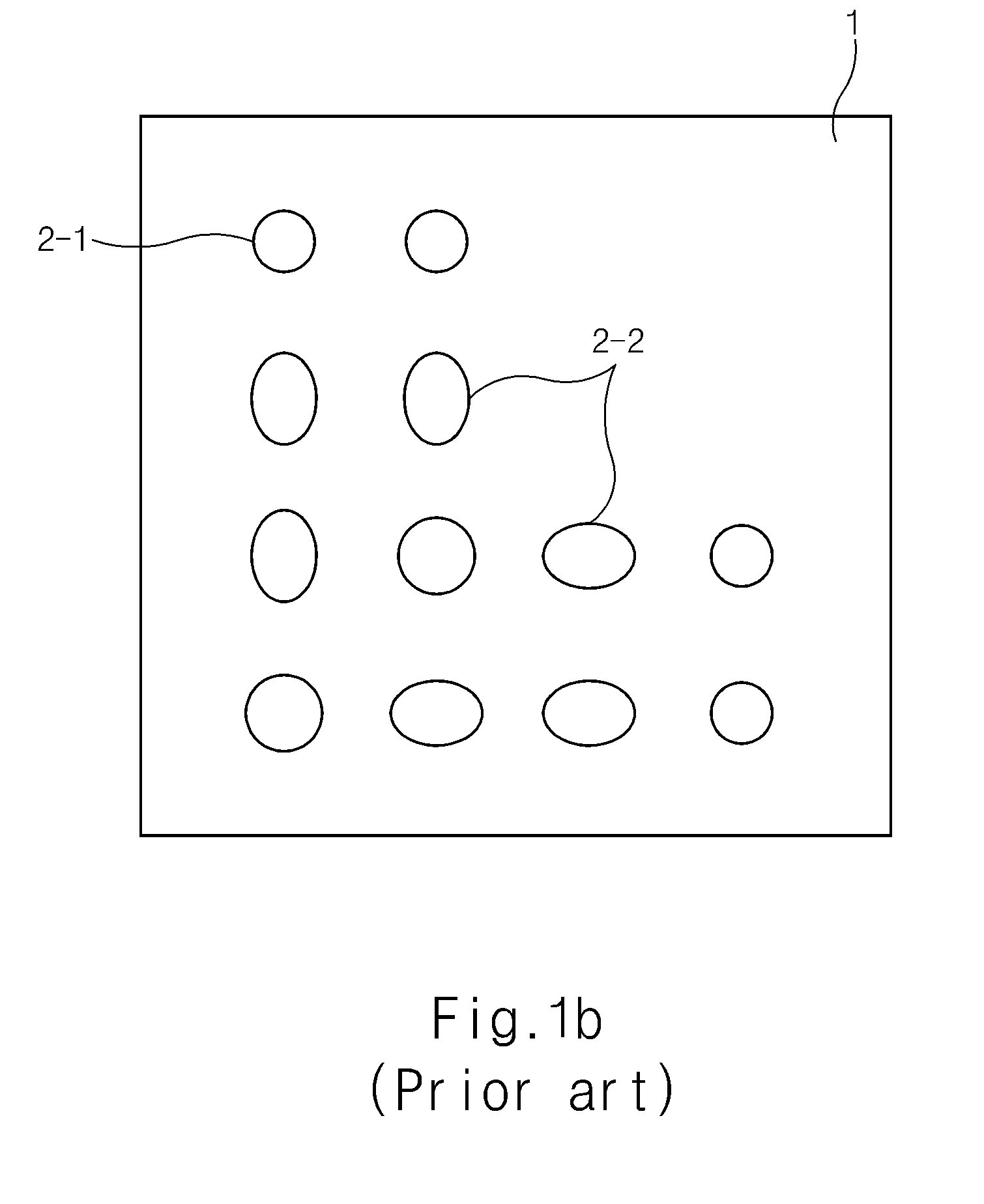
[0028]Referring to FIG. 3a, a mask film (not shown) and a first photoresist film (not shown) are formed over an underlying layer 21 of a semiconductor substrate 20 that includes lines such as a gate or bit line.

[0029]The semiconductor substrate 20 is a substrate for manufacturing a semiconductor device (e.g., a DRAM, a LOGIC device, a SRAM or a flash memory device). The substrate has lines such as a gate and a bit line. The mask film includes an amorphous carbon layer.

[0030]A first exposure mask (11) including a plurality ...


PUM

PropertyMeasurementUnit
areaaaaaaaaaaa
total areaaaaaaaaaaa
sizeaaaaaaaaaa

Abstract

A method for forming a fine contact hole of a semiconductor device comprises performing two-step etching processes using a first exposure mask including a plurality of rectangular light transmitting regions each having a given pitch and a second exposure mask including a plurality of rectangular light transmitting regions arranged a shielding region of the first exposure mask with a ‘cross (+)’ shape in the center of rectangular light transmitting regions of the second exposure mask. Each of four corner regions of the light transmitting regions of the first exposure mask is overlapped with four corner regions of rectangular light transmitting regions of the second exposure mask. As a result, the fine contact hole pattern obtained by the method has a uniform size.

Description

CROSS-REFERENCE TO RELATED APPLICATION[0001]Priority to Korean patent application number 10-2008-108447, filed on Nov. 3, 2008, the whole disclosure of which is incorporated by reference, is claimed.BACKGROUND OF THE INVENTION[0002]The invention relates to a method for forming a fine contact hole pattern of a semiconductor device.[0003]As a manufacturing technology of semiconductor devices is developed and an application field of memory devices is enlarged, a technology of manufacturing a memory device of high capacity has been required with improved integration and un-degraded electric characteristics.[0004]As a result, multilateral research has been made to improve photolithography processes, cell structures, and physical property limits of materials which form wires and insulating films.[0005]It is difficult to form a contact hole pattern of less than 50 nm using a single ArF exposure process that has a numerical aperture (NA) of less than 1.0 even though an immersion lithography...

Claims


Application Information

Patent Timeline
Patent Type & Authority Applications(United States)
IPC IPC(8): G03F1/00G03F7/20
CPCG03F7/70466G03F1/70G03F1/36G03F7/0035H01L21/76802
Inventor YUNE, HYOUNG SOON
Owner SK HYNIX INC
Why Eureka
Try Eureka