
Resistive random access memory and method for manufacturing the same

a random access memory and resistive technology, applied in the direction of basic electric elements, electrical equipment, semiconductor devices, etc., can solve the problems of scalability bottlenecks in the manufacturing of such memory, and achieve the effect of increasing resistance and reducing power consumption

Active Publication Date: 2010-05-06
MACRONIX INT CO LTD
View PDF6 Cites 230 Cited by
  • Summary
  • Abstract
  • Description
  • Claims
  • Application Information

AI Technical Summary

Benefits of technology

[0008]The invention is directed to a resistive random access memory and a method for manufacturing the same. The memory cell manufactured according to the manufacturing method of the invention without using the mask manufacturing process can break the limit of the lithography technology, hence increasing resistance and reducing power consumption.

Problems solved by technology

However, the technology for manufacturing such memory has come to a bottleneck in terms of scalability.
Currently, RRAM still has much to improve in mass production, needs to tackle with the problems of leakage current and high power consumption, and still has to overcome many other problems before commercial application matures.

Method used


Image

  • Resistive random access memory and method for manufacturing the same
  • Resistive random access memory and method for manufacturing the same
  • Resistive random access memory and method for manufacturing the same

Examples


first embodiment

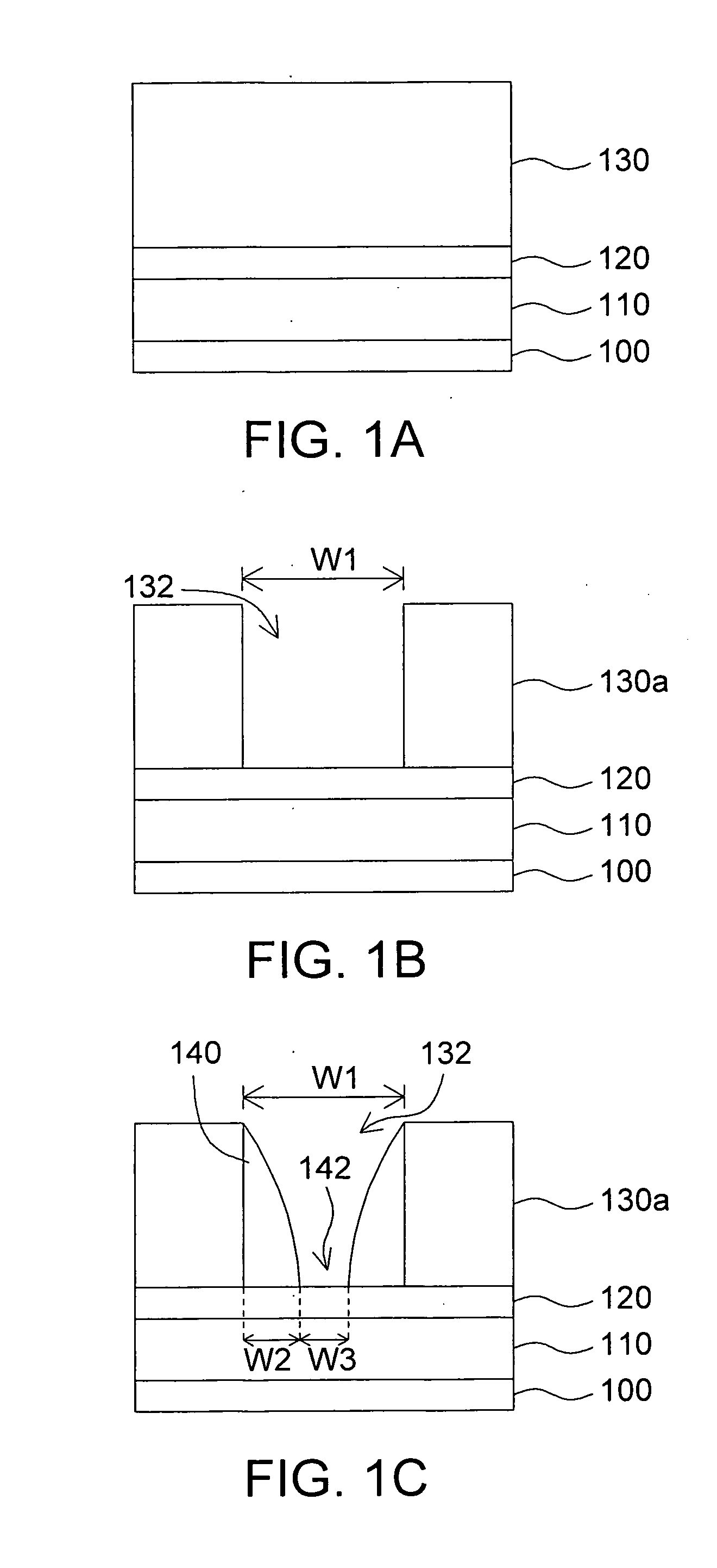
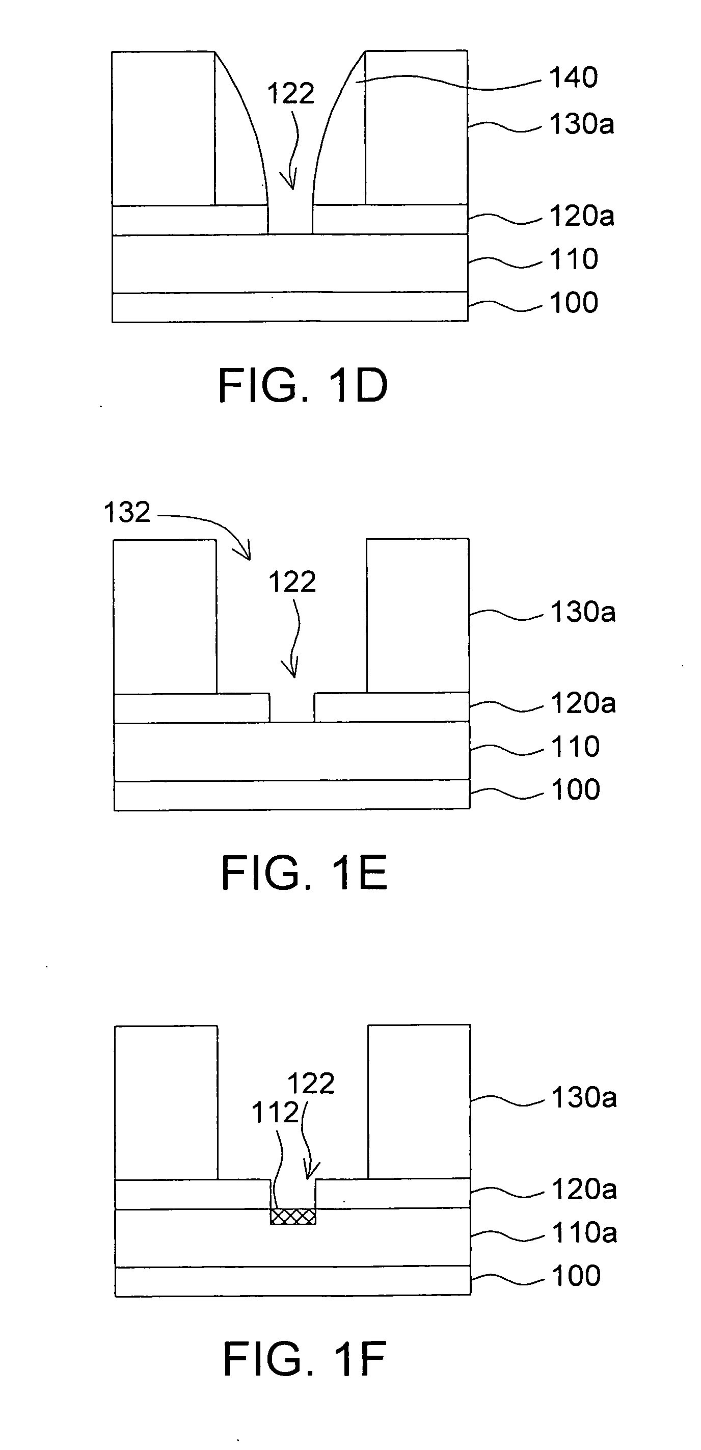
[0022]Referring to FIGS. 1A-1G, schemes showing the manufacturing process of a resistive random access memory according to a first embodiment of the invention are shown. Also referring to FIG. 2, a flowchart of the manufacturing process of a resistive random access memory according to the first embodiment of the invention is shown. Referring to FIG. 1A, first, the manufacturing process begins at step 201, a bottom electrode 110 is formed on a substrate 100, wherein the substrate 100 is a silicon wafer for example, and the bottom electrode 110 is made of aluminum-copper alloy or tungsten. Next, the manufacturing process proceeds to step 202, a nitride layer 120 is formed on the bottom electrode 110, wherein the nitride layer 120 is exemplified by silicon nitride in the present embodiment of the invention. Then, the manufacturing process proceeds to step 203, an insulating layer 130 is formed on the nitride layer 120. In the present step, silicon oxide or tetraethoxysilan (TEOS) is de...

second embodiment

[0031]Referring to FIGS. 3A-3H, schemes showing the manufacturing process of a resistive random access memory according to a second embodiment of the invention are shown. Also referring to FIG. 4, a flowchart of the manufacturing process of the resistive random access memory according to a second embodiment of the invention is shown. The steps and element characteristics of the present embodiment of the invention common to that of the first embodiment are not repeated here. Referring to FIG. 3A, the manufacturing process begins at step 401, first, a bottom electrode 310 is formed on the substrate 300. Next, the manufacturing process proceeds to step 402, an insulating layer 320 is formed on the bottom electrode 310.

[0032]Referring to FIG. 3B, as indicated in step 403, the insulating layer 320 is etched as an insulating layer 320a so as to form a contact hole 322 having a width W4.

[0033]Referring to FIG. 3C, as indicated in step 404, a conductive layer 330 is formed in the contact ho...

third embodiment

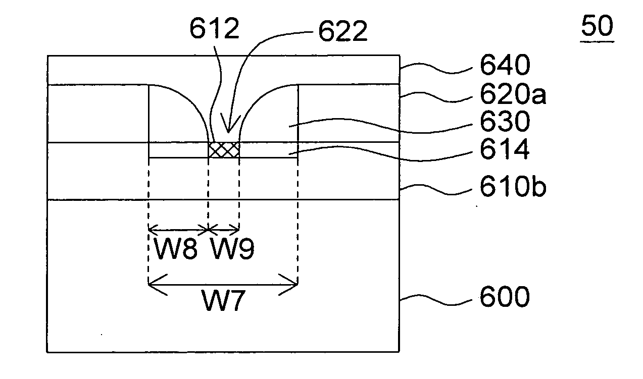
[0040]Referring to FIGS. 6A-6E, schemes showing the manufacturing process of a resistive random access memory according to a third embodiment of the invention are shown. Also referring to FIG. 7, a flowchart of the manufacturing process of a resistive random access memory according to the third embodiment of the invention is shown. The steps and element characteristics of the present embodiment of the invention common to that of the first embodiment or the second embodiment are not repeated here.

[0041]Referring to FIG. 6A, the manufacturing process begins at step 701, first, a bottom electrode 610 is formed on the substrate 600, and this bottom electrode 610 is made of tungsten. Next, the manufacturing process proceeds to step 702, an insulating layer 620 is formed on the bottom electrode 610.

[0042]Referring to FIG. 6B, as indicated in step 703, the insulating layer 620 is etched as an insulating layer 620a so as to form a contact hole 622 having a width W7.

[0043]Referring to FIG. 6...


PUM


Abstract

A resistive random access memory including, an insulating layer, a hard mask layer, a bottom electrode, a memory cell and a top electrode is provided. The insulating layer is disposed on the bottom electrode. The insulating layer has a contact hole having a first width. The hard mask layer has an opening. A portion of the memory cell is exposed from the opening and has a second width smaller than the first width. The top electrode is disposed on the insulating layer and is coupled with the memory cell.

Description

[0001]This application is a divisional application of co-pending U.S. application Ser. No. 11 / 898,529, filed Sep. 13, 2007.BACKGROUND OF THE INVENTION[0002]1. Field of the Invention[0003]The invention relates in general to a resistive random access memory and method for manufacturing the same, and more particularly to a resistive random access memory and a method for manufacturing the same capable of reducing the width of the memory cell without a mask and increasing resistance.[0004]2. Description of the Related Art[0005]Along with the advance in semi-conductor technology, electronic elements are kept being miniaturized, such that electronic products possess more and more functions when the size remains unchanged or become even smaller. As there are more and more information to be processed, the demand for the memory having larger capacity but smaller size is ever increasing.[0006]Currently, the read-write memory stores data by means of a transistor structure assisted by a memory c...

Claims


Application Information

Patent Timeline
Patent Type & Authority Applications(United States)
IPC IPC(8): H01L21/28
CPCH01L45/04H01L45/1233H01L45/1246H01L45/146H01L45/1633H10N70/828H10N70/20H10N70/028H10N70/8833H10N70/826
Inventor LEE, MING-DAOUHO, CHIA-HUALAI, ERH-KUNHSIEH, KUANG-YEU
Owner MACRONIX INT CO LTD
Learn More