Multilayered wiring board

a multi-layered wiring and wiring board technology, applied in the direction of printed circuit stress/warp reduction, conductive pattern formation, weaving, etc., can solve the problems of limited capability of conventional approach with dummy patterns to reduce board warpage, insufficient space and insufficient space secured for providing dummy patterns. to achieve the effect of reducing board warpage and restricting the provision of dummy patterns

Active Publication Date: 2010-05-13
PANASONIC CORP
View PDF20 Cites 24 Cited by
  • Summary
  • Abstract
  • Description
  • Claims
  • Application Information

AI Technical Summary

Benefits of technology

[0014]However, in the case of boards for use in compact electronic equipment which requires high-density mounting, the area occupied by lands for mounting electronic components is larger, and therefore a sufficient space cannot be secured for providing the dummy patterns. Also, in the case where components operating at high frequency are mounted on the board, formation of the dummy patterns results in generation of noise, and therefore provision of the dummy patterns is restricted. In this manner, the conventional approach with the dummy patterns is limited in its capability to reduce board warpage.
[0015]Therefore, an object of the present invention is to provide a multilayered wiring board with reduced warpage even when there is no sufficient space for providing dummy patterns on wiring layers or it is not possible to provide dummy patterns on wiring layers.

Problems solved by technology

However, in the case of boards for use in compact electronic equipment which requires high-density mounting, the area occupied by lands for mounting electronic components is larger, and therefore a sufficient space cannot be secured for providing the dummy patterns.
Also, in the case where components operating at high frequency are mounted on the board, formation of the dummy patterns results in generation of noise, and therefore provision of the dummy patterns is restricted.
In this manner, the conventional approach with the dummy patterns is limited in its capability to reduce board warpage.

Method used


Image

  • Multilayered wiring board
  • Multilayered wiring board
  • Multilayered wiring board

Examples


Embodiment Construction

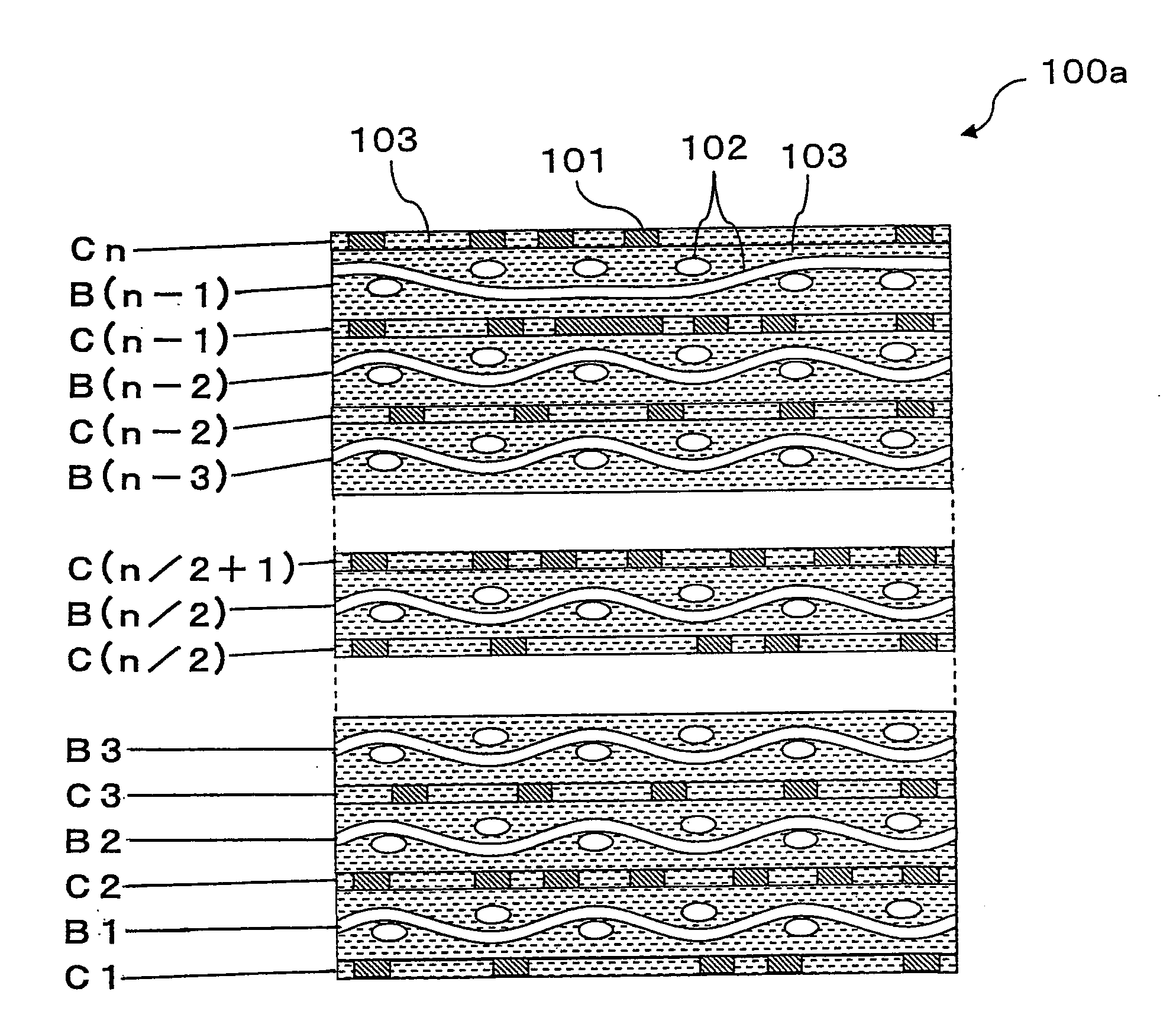
[0036]Hereinafter, a multilayered wiring board according to the present invention will be described with reference to the drawings. First, the principle for reducing warpage of the multilayered wiring board will be described.

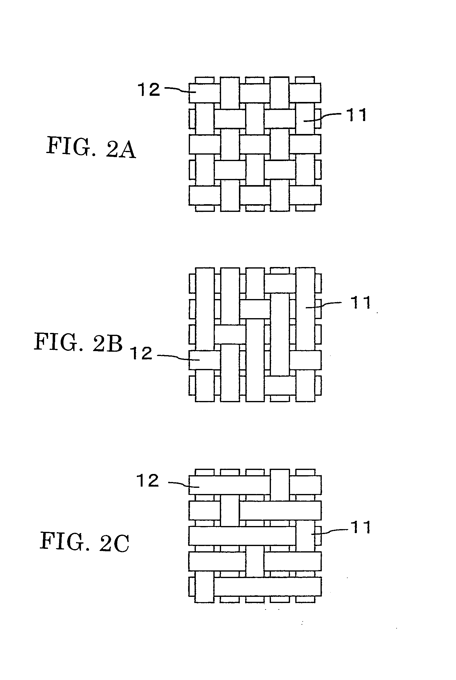
[0037]FIG. 1 illustrates a partial cross section of a multilayered wiring board 100a according to an embodiment of the present invention. In the board 100a, n (where n is an even number of 4 or more) wiring layers (C1 to Cn) and (n−1) resin base material layers [B1 to B(n−1)] are alternately laminated. The wiring layers C include copper wiring 101 and insulating resin 103. Also, the resin base material layers B include fiber bundles 102 in the form of a woven or non-woven fabric impregnated with the insulating resin 103. These structures are similar to those for the conventional board shown in FIG. 12, and elements thereof are also equal in function to those of the board. The same applies in the following description.

[0038]In the multilayered wiring board 100a, ...


PUM

PropertyMeasurementUnit
temperatureaaaaaaaaaa
radiusaaaaaaaaaa
radiusaaaaaaaaaa

Abstract

A multilayered wiring board is composed of n wiring layers and (n−1) resin base material layers, which are alternately laminated. The (n−1) resin base material layers include fiber bundles impregnated with resin. The n wiring layers include wiring patterns and resin. When half of the wiring layers in the thickness direction of the multilayered wiring board differ in the copper remaining ratio from the other half, the multilayered wiring board might be warped during heating. The crossing point density of fiber bundles in each resin base material layer is adjusted so as to cancel the warpage caused by the difference in the copper remaining ratio between the wiring layers.

Description

FIELD OF THE INVENTION[0001]The present invention relates to build-up multilayered wiring boards with two or more wiring layers.BACKGROUND OF THE INVENTION[0002]Build-up multilayered wiring boards are wiring boards developed for densely mounting various electronic components. The build-up multilayered wiring boards are used in various digital and / or mobile devices, and structured in such a manner that a plurality of wiring layers composed of copper wiring and resin and a plurality of resin base material layers composed of resin and fiber bundles are alternately laminated.[0003]First, a typical build-up multilayered wiring board will be described. FIG. 12 illustrates a partial cross section of a build-up multilayered wiring board 100g (in some cases below, simply referred to as a “board”). In the board 100g, n (where n is an even number of 4 or more) wiring layers (C1 to Cn) and (n−1) resin base material layers [B1 to B(n−1)] are alternately laminated. Hereinafter, when collectively ...

Claims


Application Information

Patent Timeline
Patent Type & Authority Applications(United States)
IPC IPC(8): H05K1/09H05K1/00
CPCH05K1/0271H05K1/0366H05K3/4688H05K2201/029H05K2201/09136Y10T442/322Y10T29/49117Y10T29/49155Y10T29/49124
Inventor OKAZAKI, TORU
Owner PANASONIC CORP
Why Eureka
Try Eureka