Multi-chip light emitting diode modules

a light-emitting diode and chip technology, applied in the field of electronic packaging, can solve the problems of affecting the emission and optical efficiency of a mcm, affecting the overall efficiency, and not having enough mass or exposed surface area to provide effective heat dissipation, so as to improve the output of luminous flux and heat dissipation, and reduce cost and complexity

Active Publication Date: 2010-05-13
CREELED INC
View PDF102 Cites 91 Cited by
  • Summary
  • Abstract
  • Description
  • Claims
  • Application Information

AI Technical Summary

Benefits of technology

[0008]The present invention provides systems and apparatuses for multi-chip lighting modules which allow for increased luminous flux output and heat dissipation in a customizable, compact package of lower cost and complexity. One embodiment comprises a multi-chip module device comprising a thermally dissipative substrate. A plurality of light emitting devices is included, and an electrically conductive layer is applied to a surface of the substrate. The conductive layer comprises a plurality of chip carrier parts each having a surface for carrying at least one of the light emitting devices. A reflective layer is also included that at least partially covers the conductive layer.

Problems solved by technology

However, a common problem with light emitting devices such as LEDs is the emitted light from the device chip is largely non-directional and non-uniform, which can negatively impact the emission and optical efficiency of a MCM.
However, for some of these devices the overall efficiency may be compromised since some of the light emitted from the multiple light sources can be absorbed is different device structure such as the substrate and spaces between the conductive and reflective pads.
However, the leads often do not have sufficient mass or exposed surface area to provide effective heat dissipation.
For example, high intensity light emitting diodes (LEDs) that emit light principally in the visible part of the electromagnetic spectrum can generate significant amounts of heat that are difficult to dissipate using such conventional techniques.
The conductive layers provided in both devices are generally insufficient to handle the necessary thermal management to prevent premature component degradation or failure, and additional means of heat dissipation, such as heat sinks, are required.
Heat sinks, however, generally take up space and increase the thickness of such devices, which can be problematic in applications in which space is at a premium.

Method used


Image

  • Multi-chip light emitting diode modules
  • Multi-chip light emitting diode modules
  • Multi-chip light emitting diode modules

Examples


Embodiment Construction

[0027]The following description presents several possible embodiments. This description is not to be taken in a limiting sense but is made merely for the purpose of describing the general principles of the invention, the scope of which is further understood by the appended claims.

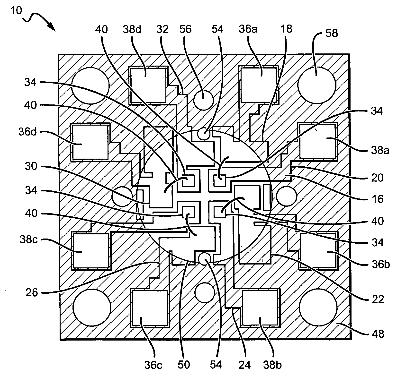
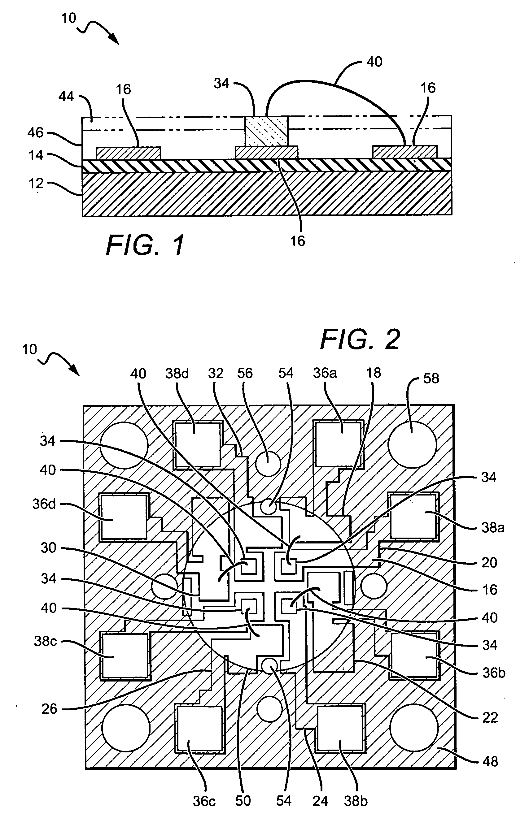
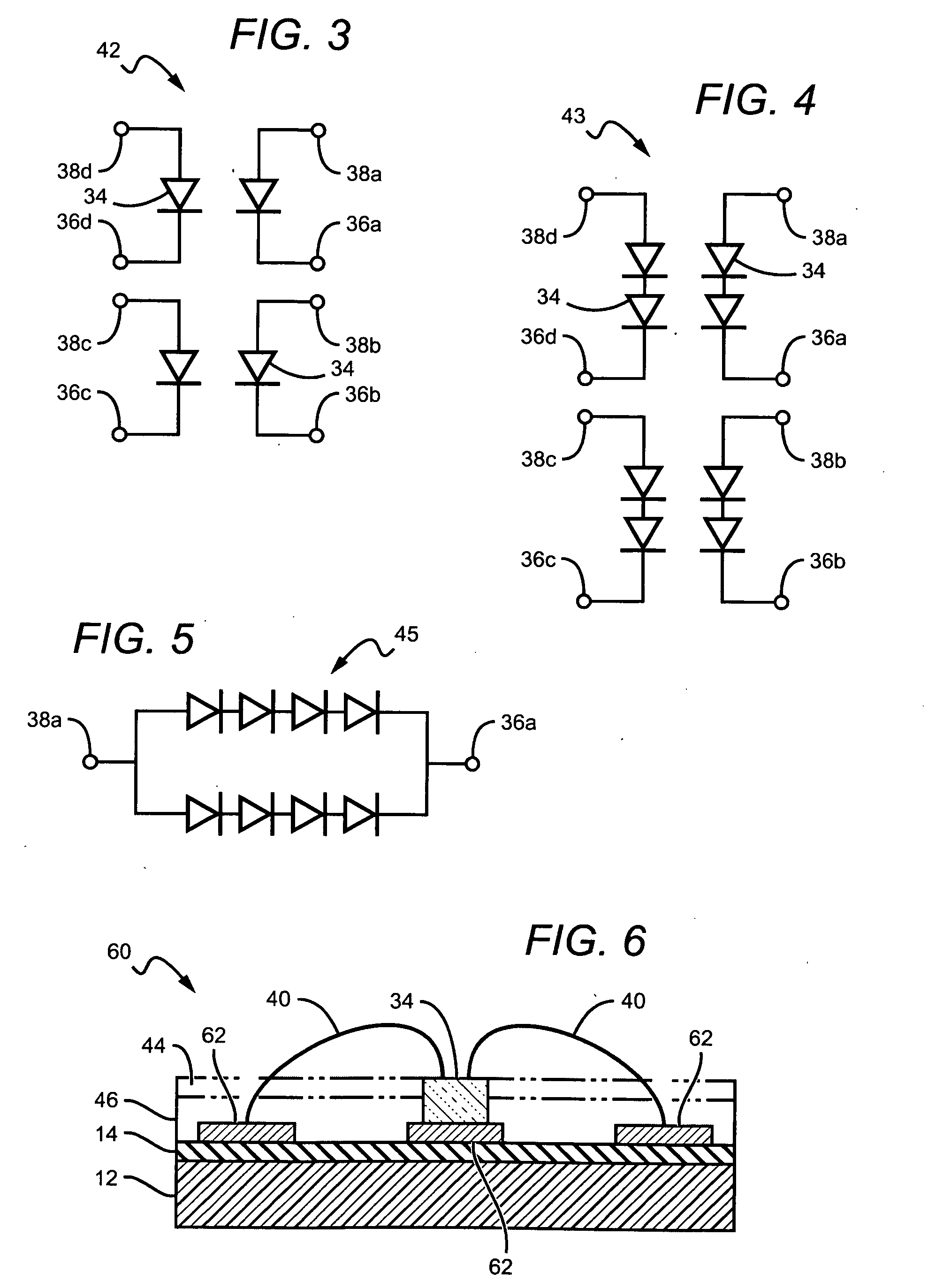
[0028]The present invention provides structures for electronic packages for light emitting devices, such as multi-chip LED modules that provide high luminous flux output, as well as improved thermal maintenance via heat dissipation. Several possible embodiments of the present invention are generally directed to multi-chip modules (MCMs) incorporating LEDs, but it is understood that other light emitting devices may also be used.

[0029]It will be understood that when an element or layer is referred to as being “on”, “connected to”, “coupled to” or “in contact with” another element or layer, it can be directly on, connected or coupled to, or in contact with the other element or layer or intervening elements or ...


PUM


Abstract

A multi-chip lighting module is disclosed for maximizing luminous flux output and thermal management. In one embodiment, a multi-chip module device comprises a substantially thermally dissipative substrate with a dark insulating layer deposited on a surface of the substrate. A plurality of light emitting devices is also provided. An electrically conductive layer is applied to a surface of the substrate, with the conductive layer comprising a plurality of chip carrier parts each having a surface for carrying at least one of the light emitting devices. Each light emitting device has a first and a second electrical terminal. A reflective layer is also provided that at least partially covers the conductive layer.

Description

BACKGROUND OF THE INVENTION[0001]1. Field of the Invention[0002]The present invention relates generally to electronic packaging, and more particularly to multi-chip modules (“MCMs” or “MCM”) for light emitting devices such as light emitting diodes (“LEDs”) and the like.[0003]2. Description of the Related Art[0004]With the advent of LEDs and other light emitting devices of increased brightness and color fidelity, multi-chip lighting modules have become available to further increase luminous flux output. MCMs for lighting typically comprise a single package with a plurality of LEDs, although it is understood that other light emitting devices may be used. Since these MCMs comprise a plurality of light emitting devices, they generally allow for high output of light emission. However, a common problem with light emitting devices such as LEDs is the emitted light from the device chip is largely non-directional and non-uniform, which can negatively impact the emission and optical efficienc...

Claims


Application Information

Patent Timeline
Patent Type & Authority Applications(United States)
IPC IPC(8): H01L33/00H01L23/48H01L21/027
CPCH01L25/0753H01L33/483H01L33/60H01L33/62H05K1/056H05K2201/0112H01L2224/48091H05K2201/10106H01L2924/00014H01L2924/00
Inventor LEUNG, JACOB CHI WING
Owner CREELED INC
Why Eureka
Try Eureka