Termination apparatus and method for planar components on printed circuit boards

Inactive Publication Date: 2010-05-13
BATTERY BIZ
View PDF8 Cites 6 Cited by
  • Summary
  • Abstract
  • Description
  • Claims
  • Application Information

AI Technical Summary

Benefits of technology

[0012]The proposed invention allows the efficient termination of a winding PCB of the planar inductive component to the main PCB, using relatively little space and providing a low-resistance connection. The disclosed methods are especially suitable for

Problems solved by technology

Effective mechanical attachment and low-resistance electrical termination (connections) of the windings to the main PCB is difficult, and consumes significant areas on both the main PCB and the winding PCB.
In addition, typical termination strategies make use of soldered connections, leading to a fundamental problem when such strategies are applied to joining planar components.
If solder does not form a concave meniscus—the solder joint is not going to be strong, and the integrity of the joint will not be reliable.
However, this proposed solution does not meet the need of having PCBs c

Method used


Image

  • Termination apparatus and method for planar components on printed circuit boards
  • Termination apparatus and method for planar components on printed circuit boards
  • Termination apparatus and method for planar components on printed circuit boards

Examples


first embodiment

Connecting a Winding PCB to a Main PCB

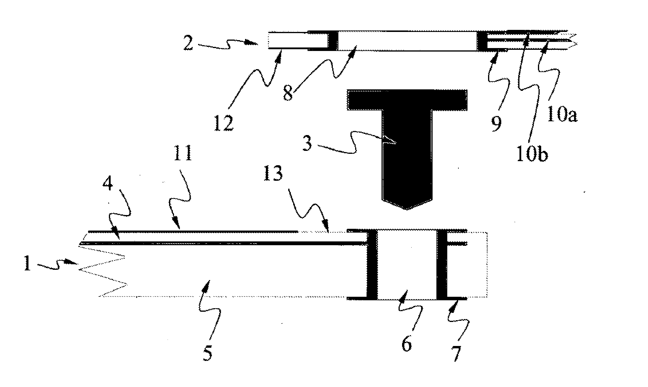
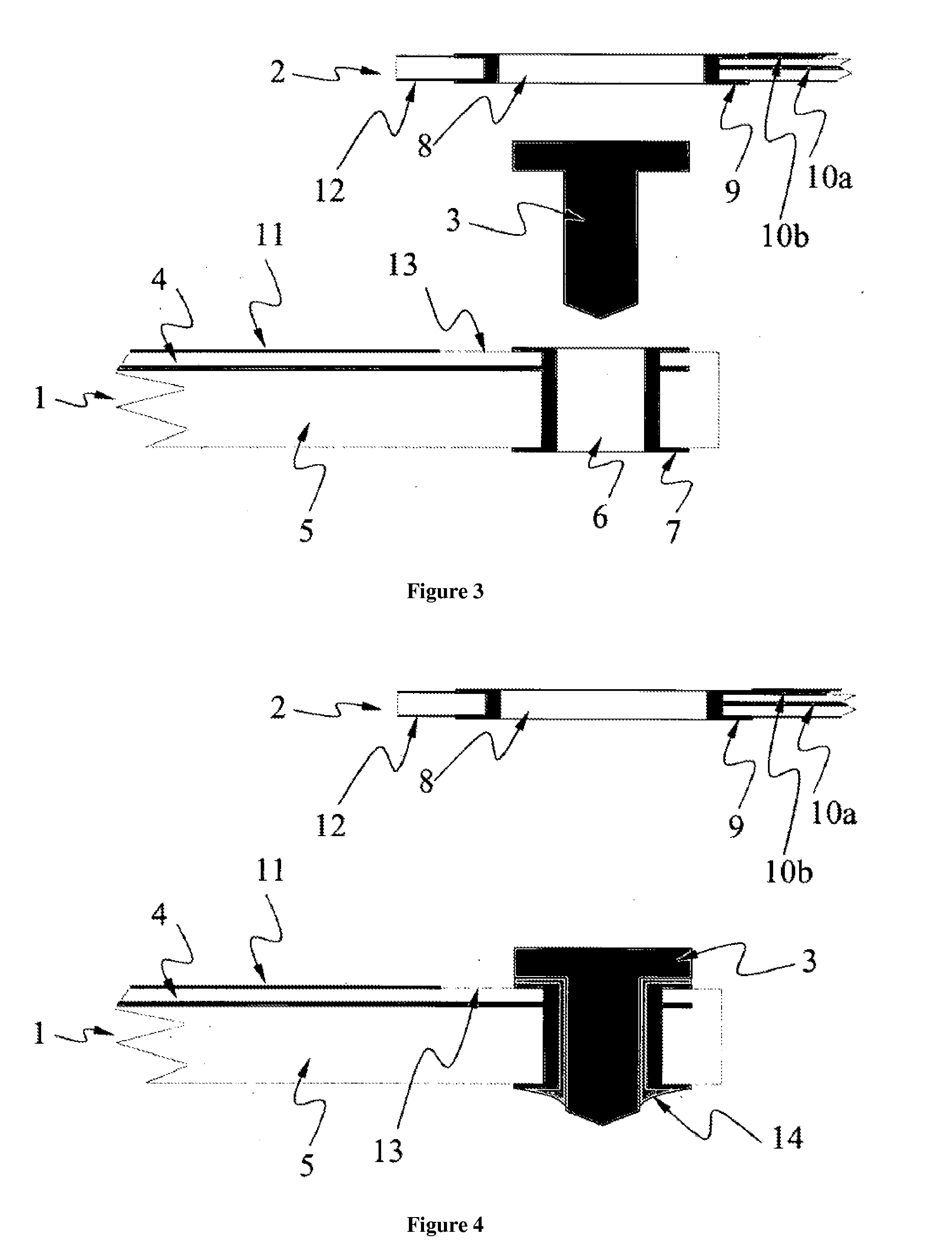
[0019]Refer to FIG. 3, which shows a winding PCB (1) (possibly of a so-called multi-layer construction), a main PCB (2) (also possibly of a so-called multi-layer construction), and a terminal pin (3). The terminal pin (3) is shown as having a “mushroom” shape, but in practice is not required to have this shape to be effective. Additionally, the terminal pin (3) is made from a solderable material; for example, copper or copper alloy.

[0020]Both the winding PCB (1) and the main PCB (2) are manufactured using established methods well-known in the industry. Each of these PCBs consists of insulating material (5), with representative copper traces (4 and 10a) embedded inside the PCB or located on the surface of the PCB (10b).

[0021]Applied on both surfaces of each PCB are so-called solder-mask layers (11 and 12). However, the solder-mask material is notably absent from the area (13) surrounding the conductive annular male ring (7) on PCB (1) around the ...

second embodiment

An Interconnected Set of PCBs With Terminations That Employ Termination Pins

[0029]This embodiment employs an interconnected set of printed circuit boards (PCBs), having a first PCB and a second PCB, said first and second PCBs configured with components needing electrical or flux coupling with components on the other of said first and second PCBs, each said PCB being constructed from insulating and non-insulating materials with conducting traces embedded inside or located on the surface of each said PCB, said PCBs coupled by at least one termination point, each said termination point comprising: a male conductive annular ring seated in said first PCB, wherein said male conductive annular ring contains a plated-through hole, and wherein the termination mating area of said first PCB immediately surrounding said male conductive annular ring is not covered with solder-mask material; a female conductive annular ring seated in said second PCB, said female conductive annular ring containing...

third embodiment

Method for Creating an Interconnected Set of PCBs With Terminations That Employ Termination Pins

[0036]This embodiment discloses a method for interconnecting a set of printed circuit boards (PCBs), having a first PCB and a second PCB, said first and second PCBs configured with components needing electrical or flux coupling with components on the other of said first and second PCBs, each said PCB being constructed from insulating and non-insulating materials with conducting traces embedded inside or located on the surface of each said PCB, said PCBs coupled by at least one termination point, each said termination point being made by the method comprising the steps of: providing a male conductive annular ring seated in said first PCB, wherein said male conductive annular ring contains a plated-through hole, and wherein the termination mating area of said first PCB immediately surrounding said male conductive annular ring is not covered with solder-mask material; providing a female cond...


PUM

PropertyMeasurementUnit
Thicknessaaaaaaaaaa
Shapeaaaaaaaaaa
Electrical conductoraaaaaaaaaa

Abstract

The disclosure involves the efficient termination of a winding PCB of a planar inductive component to a main PCB, using relatively little space and providing a low-resistance connection. The disclosed methods are especially suitable for planar structures where several winding PCBs, and/or winding PCBs and a main PCB, are all enclosed by the magnetic path components. The methods allow for a winding PCB to simply rest on the main PCB, or other winding PCBs, without any clearance. The disclosure employs mating sets of conductive annular rings with an optional interlocking terminal pin that allows two PCBs to be fixedly coupled together, while preserving a minimum distance between the solder-mask layers of the two PCBs in order to prevent the formation of unwanted electrical connections between the two PCBs. Solder is used to ensure effective coupling in each assembly of mating annular rings and optional terminal pin.

Description

CROSS-REFERENCE TO RELATED APPLICATIONS[0001]This application claims priority from U.S. application Ser. No. 60 / 997,633, filed Oct. 5, 2007, which application is incorporated herein by reference for all purposes.BACKGROUND OF THE INVENTION[0002]The preferred power-conversion method for modern electronic equipment is the Switching Mode Power Supply (SMPS). It is characterized by high efficiency and resulting low wasted heat dissipation.[0003]In order to create the SMPS circuit, various inductive components are required. As modern electronic devices shrink in dimensions, correspondingly all inductive components must be reduced in size. One method for achieving this reduction in size is to use so-called planar inductive structures, where the magnetic-path components (core) are snapped around flat windings incorporated into the printed-circuit board (PCB). A PCB may actually be carrying all components of the device (main PCB). More commonly, however, a PCB carrying an inductive componen...

Claims


Application Information

Patent Timeline
IPC IPC(8): H05K1/11H05K3/36
CPCH05K1/165H05K3/3447H05K3/363H05K3/368H05K2201/096Y10T29/49165H05K2201/10666H05K2201/10871Y10T29/49153Y10T29/49126H05K2201/10303
Inventor MARTEN, VICTORPATEL, AAKARVANSTONE, MARK
Owner BATTERY BIZ
Why Eureka
Try Eureka