Semiconductor device and method for manufacturing the same
a semiconductor and semiconductor technology, applied in the field of semiconductor devices, can solve problems such as insufficient characteristics, and achieve the effect of excellent semiconductor devices and improved electrical characteristics of oxide semiconductors
- Summary
- Abstract
- Description
- Claims
- Application Information
AI Technical Summary
Benefits of technology
Problems solved by technology
Method used
Image

Examples
embodiment 1
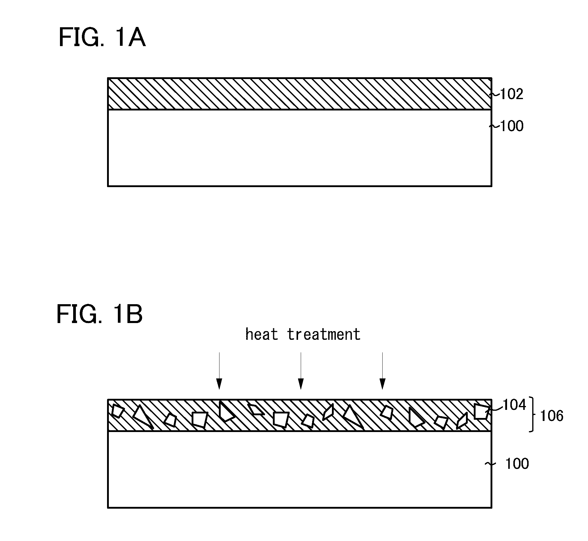
[0037]In this embodiment, a method for manufacturing an oxide semiconductor layer in which crystal grains represented by InGaO3(ZnO)m (m=1) are included in an amorphous structure represented by InGaO3(ZnO)m (m>0) (the oxide semiconductor layer is referred to as an In—Ga—Zn—O based oxide semiconductor layer) is described with reference to drawings.
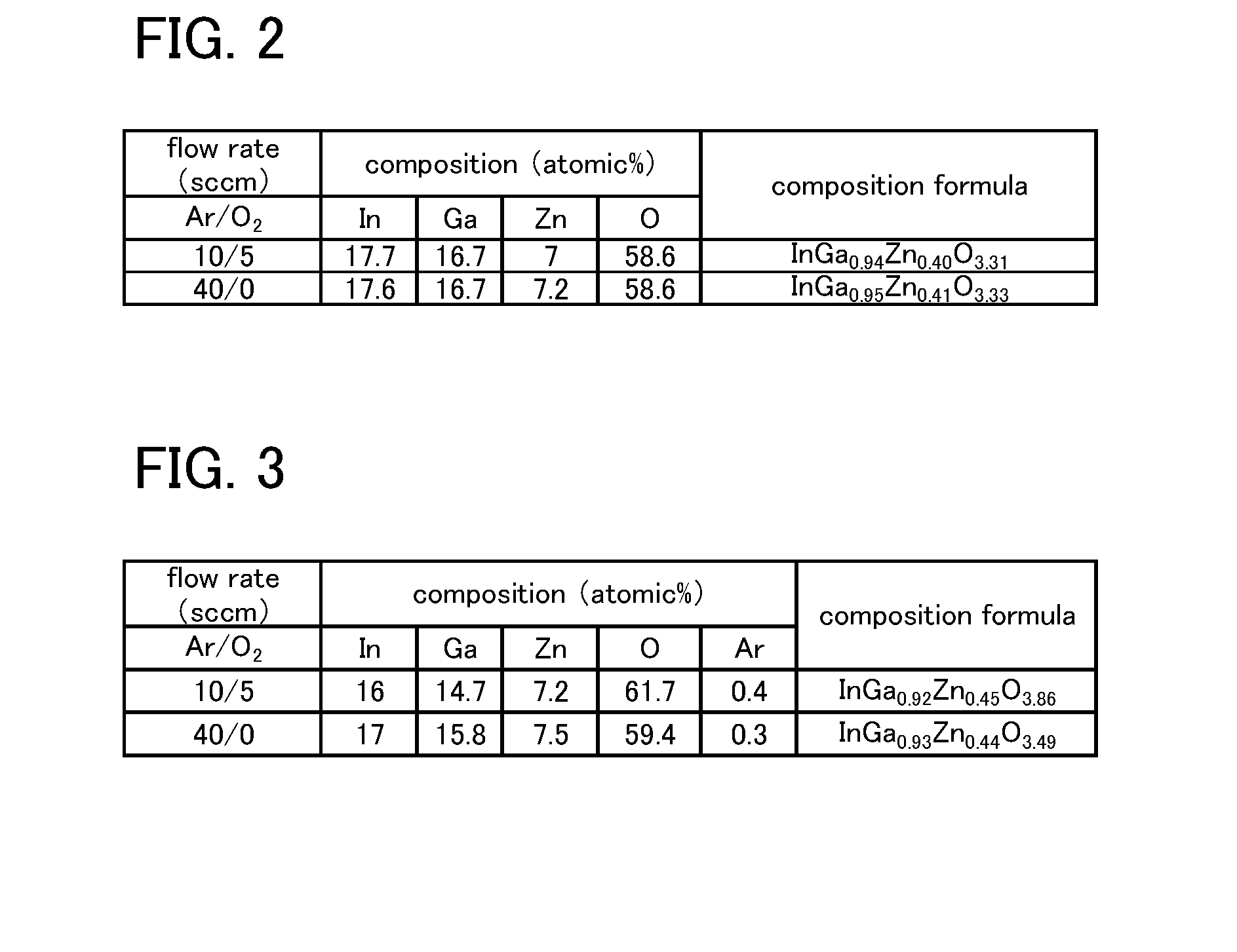
[0038]First, an In—Ga—Zn—O based non-single-crystal semiconductor layer 102 is formed over a formation surface (here, over a substrate 100) (see FIG. 1A). For example, the non-single-crystal semiconductor layer 102 can be formed by a sputtering method using an oxide semiconductor target including indium (In), gallium (Ga), and zinc (Zn). For example, the following conditions may be employed for the sputtering: a distance between the substrate 100 and the oxide semiconductor target is 30 mm to 500 mm; the pressure is 0.1 Pa to 2.0 Pa; the DC power source is 0.2 kW to 5.0 kW (when the target with a size of 8-inch in diameter is used); and the...
embodiment 2
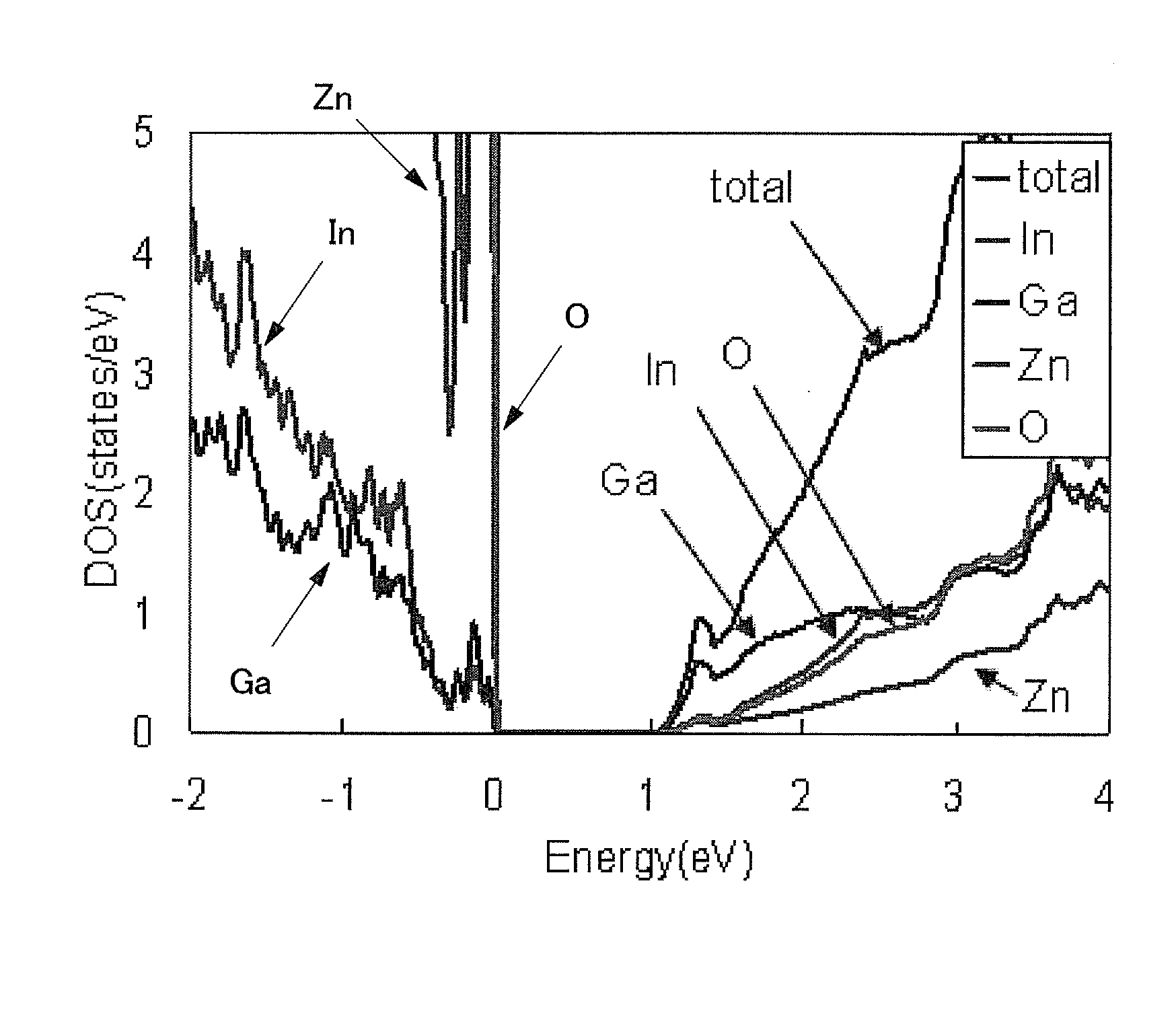
[0074]In this embodiment, the result of promoting the consideration of an In—Ga—Zn—O based oxide semiconductor layer in Embodiment 1 is described with reference to drawings.
[0075]It is revealed in Embodiment 1 that two (Ga, Zn)O2 layers and one InO2 layer are included in a unit cell of a crystal structure of InGaZnO4. In response to this, the distribution of Ga atoms and Zn atoms is studied in more detail in this embodiment. In specific, some combinations of an upper layer and a lower layer are given as shown in FIGS. 9A and 9B, and the relation between the distribution of Ga atoms and Zn atoms in two (Ga, Zn)O2 layers and the energy is calculated and considered.
[0076]FIGS. 14A to 14D illustrate specific combinations (the distributions of atoms) which are subjected to calculation. In this embodiment, these combinations are selected with a focus on the number of nearest neighbor atoms of the same kind. For example, in a combination shown in FIG. 14A, Ga atoms and Zn atoms are distrib...
embodiment 3
[0080]In this embodiment, an example of a manufacturing process of a semiconductor device using an oxide semiconductor layer manufactured by the method described in Embodiment 1 or the like is described with reference to FIGS. 17A to 17E. Note that in this embodiment, the detailed description of the content which is the same or substantially the same as in Embodiment 1 or the like is omitted.
[0081]First, a gate electrode 202 is formed over a substrate 200 having an insulating surface, and a gate insulating layer 204 is formed over the gate electrode 202; then, an oxide semiconductor layer 206 and an oxide semiconductor layer 207 are stacked (see FIG. 17A).
[0082]As the substrate 200 having an insulating surface, for exmaple, a glass substrate having a visible light transimitting property, which is used for a liquid crystal display device or the like, can be used. The glass substrate is preferably an alkali-free glass substrate. As an alkali-free glass substrate, for example, a glass ...
PUM
 Abstract
Description
Claims
Application Information
 - Generate Ideas
- Intellectual Property
- Life Sciences
- Materials
- Tech Scout
- Unparalleled Data Quality
- Higher Quality Content
- 60% Fewer Hallucinations
Browse by: Latest US Patents, China's latest patents, Technical Efficacy Thesaurus, Application Domain, Technology Topic, Popular Technical Reports.
© 2025 PatSnap. All rights reserved.Legal|Privacy policy|Modern Slavery Act Transparency Statement|Sitemap|About US| Contact US: help@patsnap.com