Configurable architecture hybrid analog/digital delay locked loop (DLL) and technique with fast open loop digital locking for integrated circuit devices

a technology of digital locking loop and configuration architecture, applied in the direction of digital storage, pulse automatic control, instruments, etc., can solve the problem of proving more difficult to achieve the same timing resolution per stage for digital locking with such a delay line design

Active Publication Date: 2010-05-20
PROMOS TECH INC
View PDF3 Cites 13 Cited by
  • Summary
  • Abstract
  • Description
  • Claims
  • Application Information

AI Technical Summary

Benefits of technology

[0006]Disclosed herein is a configurable architecture, hybrid analog / digital delay locked loop and technique with fast open loop digital locking for integrated circuit dynamic random access memory (DRAM) devices and devices incorporating embedded DRAM. The DLL design and technique disclosed herein employs a hybrid analog / digital delay line, but does not use a conventional closed loop architecture during the digital phase of the locking process.
[0007]In a preferred embodiment of the present invention, the first portion of the delay line has analog delay stages while the second portion of the delay line has fixed delay stages with tap outputs available at each delay stage. The appropriate tap for locking the DLL is digitally selected. A novel feature of the present invention is that the circuit blocks are configured as an open loop architecture for adjusting the number of stages (selecting the appropriate tap) in the digital portion of the delay line to achieve a locked condition, rather than the traditional closed loop architecture. In operation, the circuit blocks are re-configured as a traditional closed loop DLL architecture for the analog fine-tuning. While the hybrid delay line may also comprise all analog delay stages with taps at each stage, it may prove more difficult to achieve the same timing resolution per stage for digital locking with such a delay line design.
[0008]Particularly disclosed herein is an integrated circuit device including a analog / digital delay locked loop that may be configured as an open loop or a closed loop that comprises an input buffer to receive a clock signal. The input buffer output is connected to a single narrow edge pulse generator, a narrow reference pulse stream generator, and, selectively, to a combination analog / digital variable delay line with output taps at each stage of the digital portion thereof. Tap select logic receives the narrow reference pulse stream and the output taps from the digital portion of the delay line. The output taps are also inputs to a multiplexing circuit (MUX) whose output is, selectively, input to a replica delay line and an output data path. The output of the single narrow edge pulse generator is, selectively, connected to the input of the replica delay line and the output data path. The final tap of the digital delay line is input to an end detect latch. The output of the input buffer is further connected to the input of a phase detector whose other input is the output of the replica delay line. The output of the replica delay line is further connected to a dummy multiplexer. The output of the dummy multiplexer is connected, selectively, to the input of the delay line. Two outputs of the phase detector are inputs to a voltage control generator that provides control voltages as outputs to control the delay per stage of the analog portion of the delay line. An analog reset circuit receives one output of the end detect latch and the output of the input buffer and has its output connected to the phase detector and the control voltage generator. The term “selectively” is used herein with reference to configuration logic that selectively steers the respective signals to the denoted subsequent inputs based on the state of the end detect latch.
[0009]Also particularly disclose herein is a method for operating an analog / digital delay locked loop, that may be configured as an open loop or a closed loop, in an integrated circuit device which comprises, in the open loop configuration, supplying a clock signal to an input buffer. The input buffer is coupled to a narrow reference pulse stream generator and a narrow single edge pulse generator. The narrow edge pulse generator is coupled selectively to a replica delay line whose output is selectively coupled to the input of dummy multiplexer whose output is selectively coupled to a variable delay line comprising analog and digital portions thereof, the digital portion having output taps at each stage of delay. The single narrow pulse generated propagates down the enabled path and appears at each output tap of the digital portion of the variable delay line in turn. The narrow reference pulse stream generator is coupled to tap select logic that also receives the output taps from the digital portion. The tap select logic compares the single narrow pulse output signals appearing at the output taps in sequence to the narrow reference pulse stream and selects the output tap most closely aligned to a reference pulse, thus performing the initial digital locking. When the single narrow pulse reaches the end of the analog / digital delay line it sets an end detect latch that is initially reset, causing the delay locked loop to be re-configured as a closed loop. The analog / digital delay line also comprises, in the closed loop configuration, supplying a clock signal to an input buffer coupled selectively to the variable delay line and a phase detector. The output of the variable delay line is coupled to the replica delay line, which is coupled to the other input of the phase detector. The phase detector is coupled to a control voltage generator. The control voltage generator is coupled to the analog portion of the delay line and adjusts the delay per stage of the analog portion of the delay line in response to the signals coupled from the phase detector thus performing the analog locking.

Problems solved by technology

While the hybrid delay line may also comprise all analog delay stages with taps at each stage, it may prove more difficult to achieve the same timing resolution per stage for digital locking with such a delay line design.

Method used


Image

  • Configurable architecture hybrid analog/digital delay locked loop (DLL) and technique with fast open loop digital locking for integrated circuit devices
  • Configurable architecture hybrid analog/digital delay locked loop (DLL) and technique with fast open loop digital locking for integrated circuit devices
  • Configurable architecture hybrid analog/digital delay locked loop (DLL) and technique with fast open loop digital locking for integrated circuit devices

Examples


Embodiment Construction

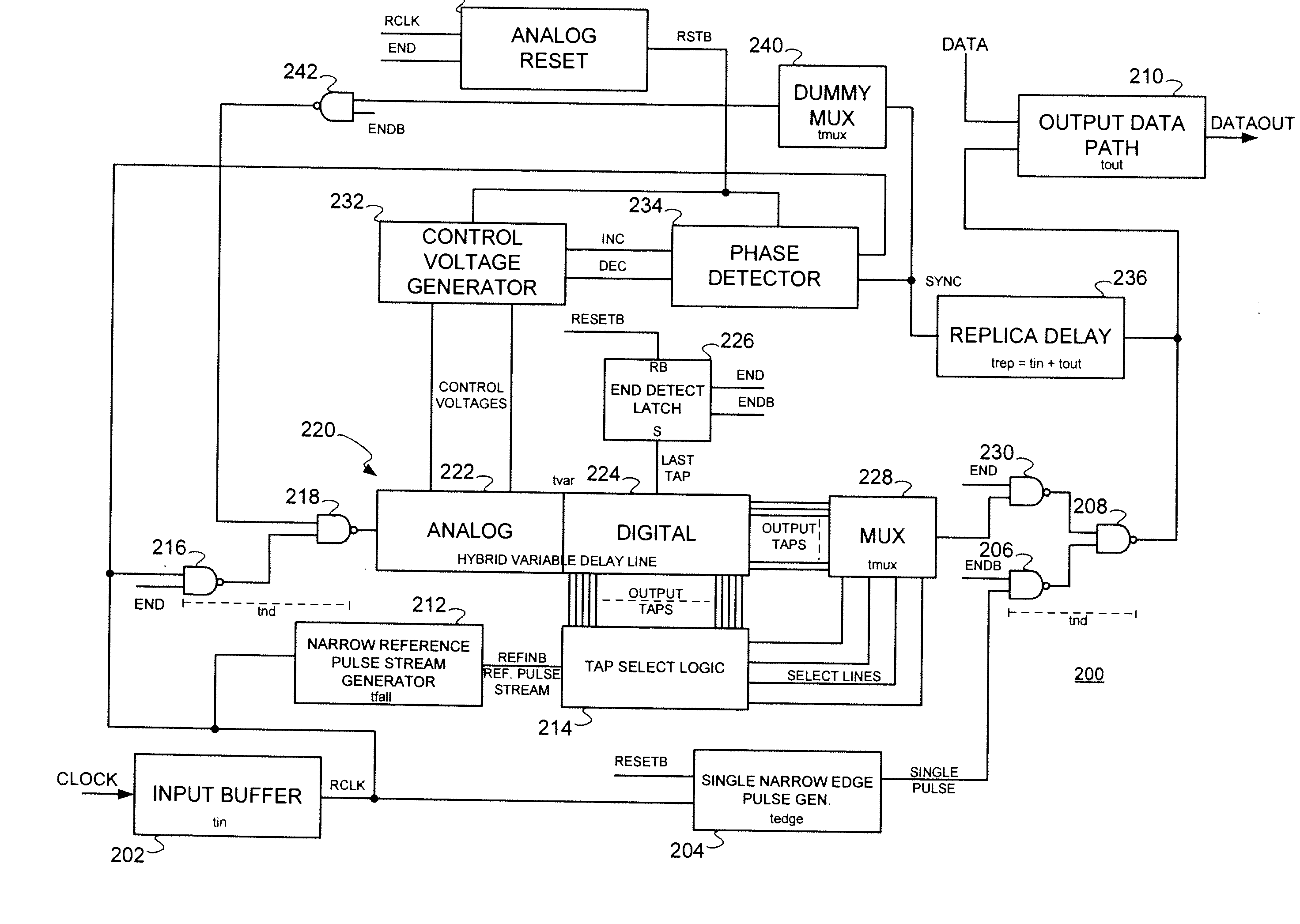
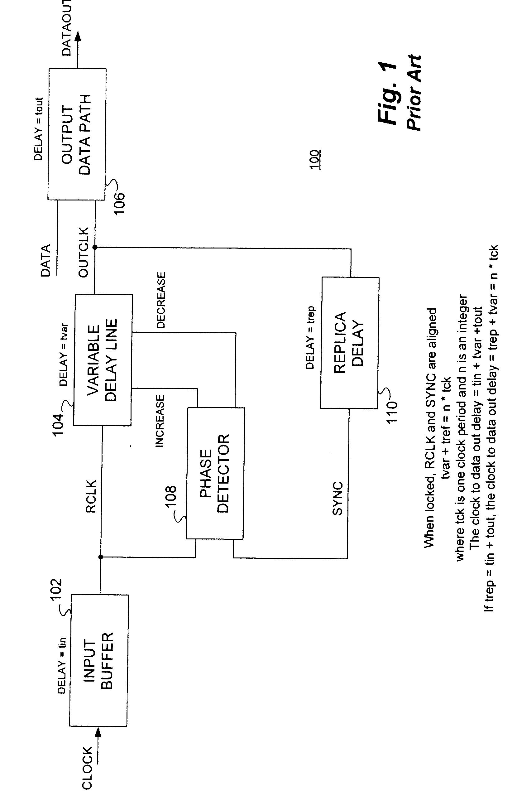
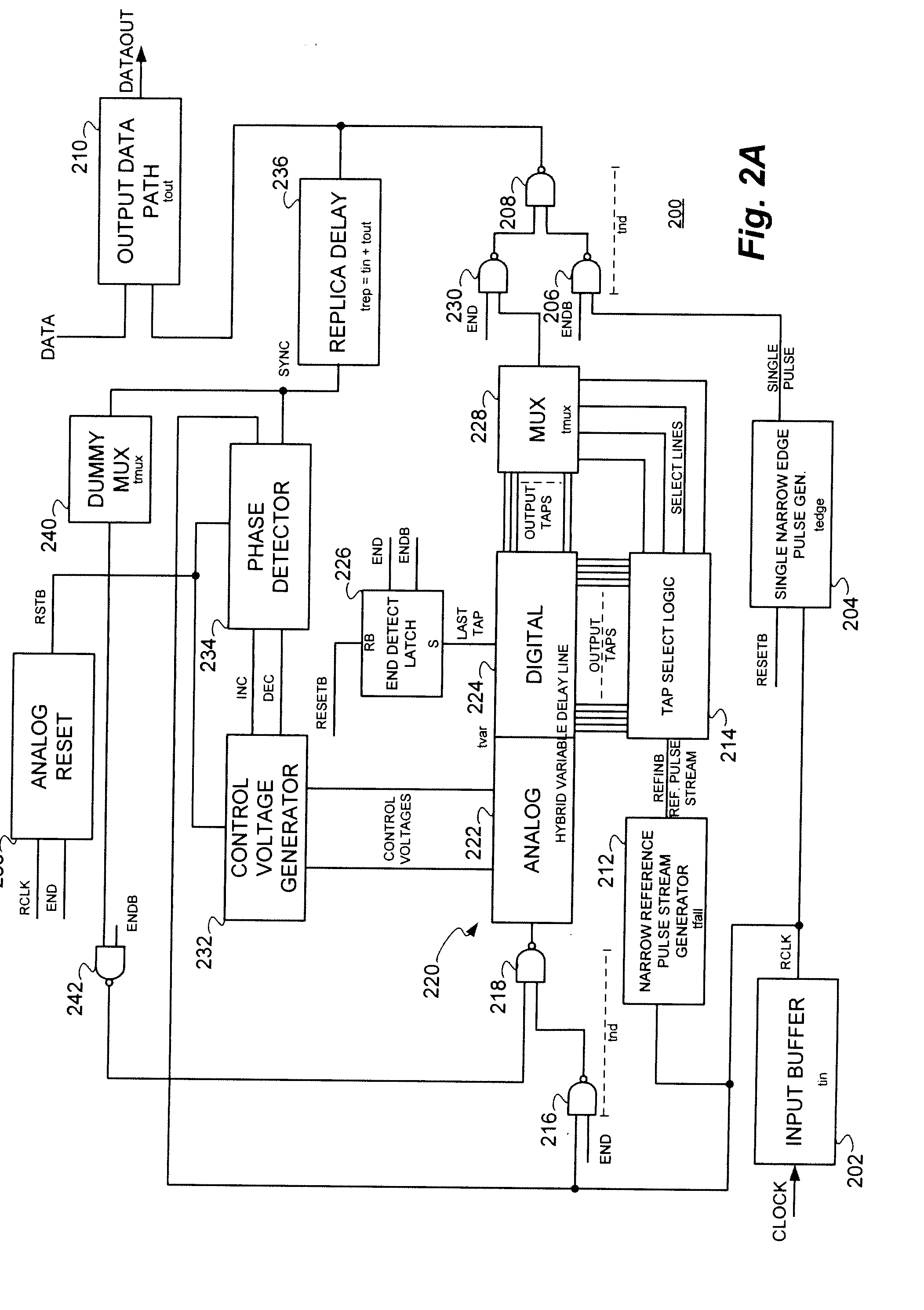
[0019]With reference now to FIG. 1, a simplified functional block diagram of a conventional prior art DLL 100 design implemented in the form of a closed loop architecture is shown. The conventional DLL 100 comprises an input buffer 102 which receives a system clock signal (CLOCK) input to produce a buffered clock signal (RCLK) output and has a delay “tin”. The RCLK signal is supplied as an input to a variable delay line 104 to produce an OUTCLK signal which is input to an output data path 106 in addition to a data input to provide the aligned DATAOUT signal as shown. The variable delay line 104 has a delay of “tvar” while the output data path 106 has a delay of “tout”.

[0020]A phase detector 108 also receives the buffered clock signal RCLK as well as a feed back signal (SYNC) output from a replica delay block 110 which receives the OUTCLK signal as an input. The replica delay block 110 has a delay of “trep”. The phase detector 108 provides an INCREASE or DECREASE signal to the variab...


PUM


Abstract

A configurable architecture, hybrid analog/digital delay locked loop and technique with fast open loop digital locking for integrated circuit dynamic random access memory (DRAM) devices and devices incorporating embedded DRAM. The DLL design and technique disclosed employs a hybrid analog/digital delay line, but does not use conventional closed loop architecture during the digital phase of the locking process.

Description

BACKGROUND OF THE INVENTION[0001]The present invention relates, in general, to the field of integrated circuit devices. More particularly, the present invention relates to a configurable architecture, hybrid analog / digital delay locked loop and technique with fast open loop digital locking for integrated circuit dynamic random access memory (DRAM) devices and devices incorporating embedded DRAM.[0002]Delay Locked Loops (DLLs) are used in semiconductor memory devices to align the output data with the system clock. In conventional DLL designs for memory devices, a phase detector is utilized to compare the rising edges of a buffered system clock with a feedback signal in order to adjust the delay of a variable delay line until the rising edges of the two signals are aligned. In operation, if a replica delay in the feedback path of the DLL exactly matches the sum of the input buffer and output data path delays, the output data will then be aligned with the input clock since the delay be...

Claims


Application Information

Patent Timeline
Patent Type & Authority Applications(United States)
IPC IPC(8): H03L7/06
CPCG11C7/1051G11C7/1066G11C7/22H03L7/10H03L7/0812H03L7/0814G11C7/222H03L7/0816
Inventor HEIGHTLEY, JOHN D.
Owner PROMOS TECH INC
Why Eureka
Try Eureka