Printed circuit board and optical transmission device

Active Publication Date: 2010-05-20
LUMENTUM JAPAN INC
View PDF6 Cites 11 Cited by
  • Summary
  • Abstract
  • Description
  • Claims
  • Application Information

AI Technical Summary

Benefits of technology

[0013]According to still another aspect of the present invention, the plurality of the trap filters have a distance between respective via holes thereof set to equal to or less than ¼ a wavelength of the clock signal. With this structure, it is possible to effectively attenuate a noise having a wavelength of the clock signal.
[0014]According to a further aspect of the present invention, the plurality of the trap filters have a distance between respective via holes thereof set to equal to or less than 0.3 mm. With this structure, it is possible to effectively attenuate a noise due to the clock signal at a clock frequency of equal to or higher than 20 GHz.
[0015]According to a further aspect of the present invention, the plurality of the trap filters have mutually different frequency components to be attenuated. With this structure, it is possible to attenuate a noise within a frequency band including the frequency of the clock signal.
[0016]According to a further aspect of the present invention, the signal output circuit includes: an oscillator circuit for oscillating a clock signal; and an amplifier circuit for amplifying the clock signal oscillated by the oscillator circuit, and the trap filter is provided to the power supply wiring for each of the oscillator circuit and the amplifier circuit. With this structure, i

Problems solved by technology

However, the above-mentioned conventional technology may appropriately reduce the unintentional electromagnetic wave in a frequency range of from approximately 30 MHz to 1 GHz, but may not obtain a sufficient effect of reducing a high-frequency noise component, which is generated when handling a signal having a high frequency of, for example, equal to or higher than 20 GHz, which is used in a case of

Method used


Image

  • Printed circuit board and optical transmission device
  • Printed circuit board and optical transmission device
  • Printed circuit board and optical transmission device

Examples


first embodiment

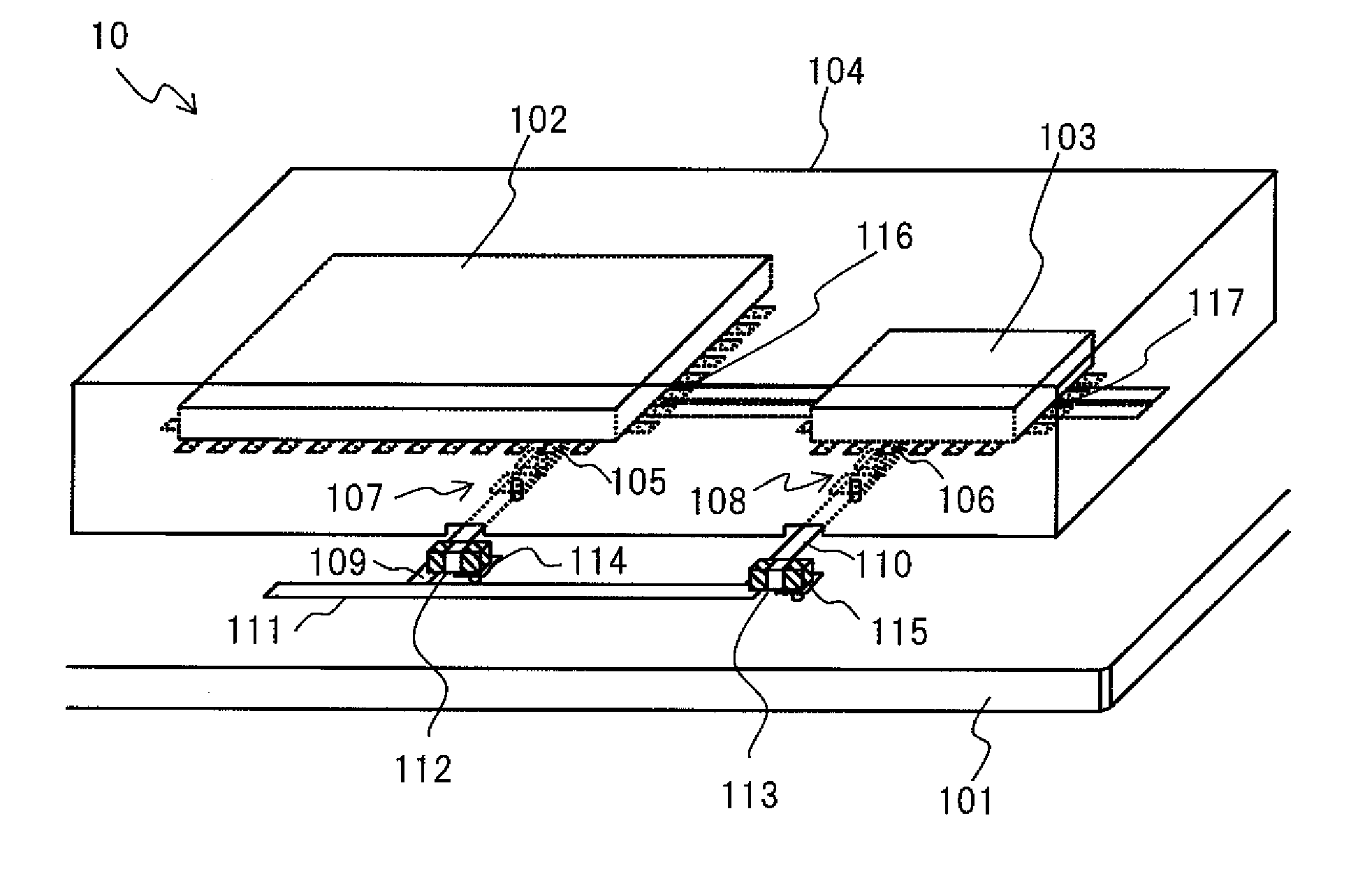
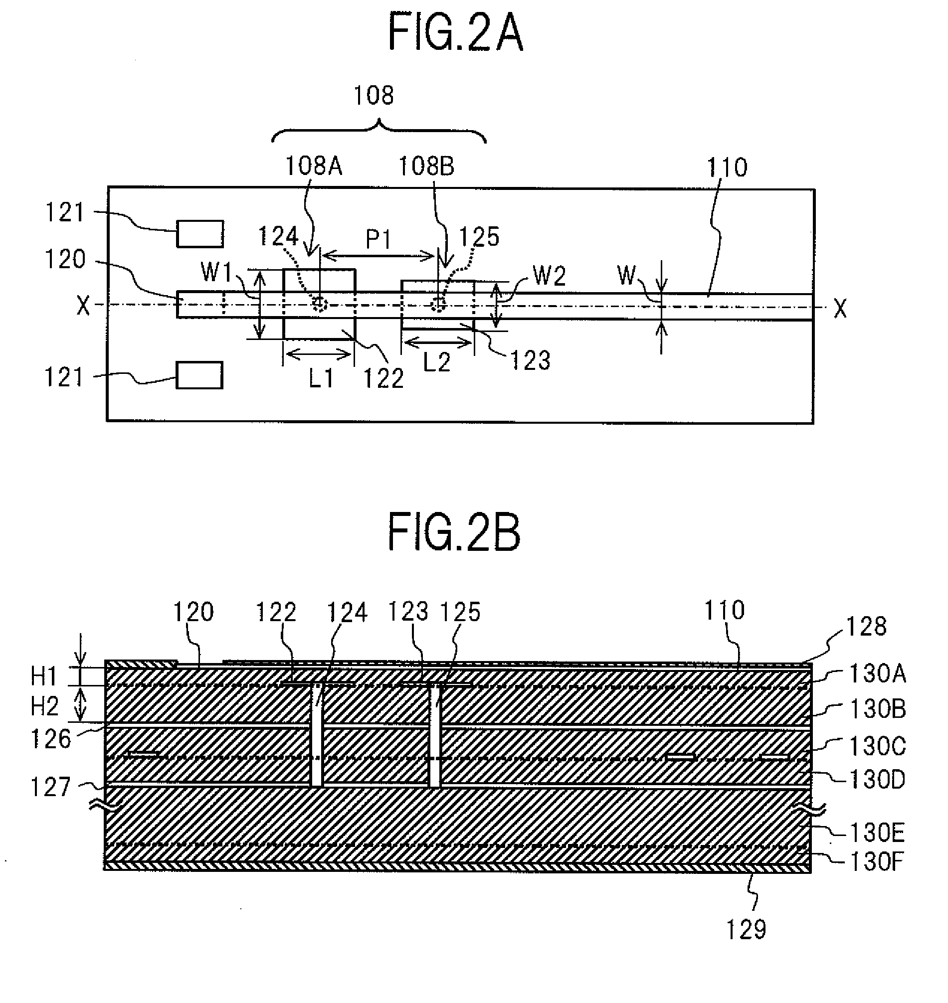
[0042]First, FIGS. 2A and 2B are structural diagrams illustrating the trap filter according to the FIGS. 2A and 2B illustrate only the structure of the trap filter 108, but the trap filter 107 has the same structure. FIG. 2A illustrates a part of the substrate 101 in which the trap filter 108 is formed, which is viewed from above, and FIG. 2B is a cross-sectional view thereof along the line X-X of FIG. 2A.

[0043]As illustrated in FIGS. 2A and 2B, the trap filter 108 includes two resonance circuits arranged in series in the power supply wiring 110. A first resonance circuit 108A includes one region of the power supply wiring 110 formed of a surface-layer wiring provided to a surface of the substrate 101, a minute isolated pattern 122 formed of a first inner-layer wiring located below the one region, and a via hole 124 that connects the minute isolated pattern 122 and a ground wiring layer 126 formed of a second inner-layer wiring.

[0044]A second resonance circuit 108B includes one reg...

second embodiment

[0058]Next, as illustrated in FIG. 6, the line (4) of the conventional technology provided with no trap filter indicates that the maximum electric field intensity is equal to or larger than 90 dB (μV / m) in a frequency range from the frequency of 19 GHz to the frequency of 21.6 GHz, while the line (2) of the second embodiment indicates that the maximum electric field intensity of the unintentional electromagnetic wave is successfully reduced to equal to or smaller than 70 dB (μV / m) in the same frequency range. In other words, FIG.

[0059]6 indicates that the second embodiment produces an effect of such a great improvement that the unintentional electromagnetic wave is cut by equal to or larger than 20 dB in the domain of a frequency bandwidth of 2.6 GHz including the clock signal frequency of 21.5 GHz.

third embodiment

[0060]Further, as illustrated in FIG. 6, the line (3) of the third embodiment indicates that the maximum electric field intensity of the unintentional electromagnetic wave is successfully reduced to equal to or smaller than 70 dB (μV / m) at the frequency of 20.6 GHz.

[0061]The impedance at a tip of the power supply wiring 110 may vary from 0Ω (short: short-circuited) to infinity (open: open-circuited) depending on a circuit layout or a frequency, and the unintentional electromagnetic wave needs to be reduced in all of the cases. Therefore, FIG. 7 illustrates changes of the unintentional electromagnetic wave intensities in a case where a tip impedance of the power supply wiring 110 is caused to change at the frequency of 20.6 GHz at which the maximum reduction effects are obtained in FIG. 6. In FIG. 7, the line (1) represents the first embodiment, the line (2) represents the second embodiment, the line (3) represents the third embodiment, and the line (4) represents the conventional te...


PUM


Abstract

To reduce emission of an unintentional electromagnetic wave even if a frequency of a clock signal being output is high, a printed circuit board (10) includes: a substrate (101); signal output circuits (102 and 103) formed on the substrate (101), for outputting a clock signal; power supply wirings (109 and 110) for connecting the signal output circuits (102 and 103) and a power source; and trap filters (107 and 108) provided to the power supply wirings (109 and 110), for attenuating a frequency component corresponding to a frequency of the clock signal.

Description

CROSS-REFERENCE TO RELATED APPLICATION[0001]The present application claims priority from Japanese application JP2008-293947 filed on Nov. 17, 2008, the content of which is hereby incorporated by reference into this application.BACKGROUND OF THE INVENTION[0002]1. Field of the Invention[0003]The present invention relates to a printed circuit board and an optical transmission device.[0004]2. Description of the Related Art[0005]There is a demand to reduce an intensity of an unintentional electromagnetic wave generated from an optical transmission device to lower than a predetermined value. As the optical transmission device has many electromagnetic waves radiated from a built-in IC, development of a technology for effectively reducing the electromagnetic waves radiated from the IC becomes important.[0006]To cope with this, JP 2970660 B proposes a technology for reducing the radiation of an unintentional electromagnetic wave due to a switching noise from an IC through arrangement of two ...

Claims


Application Information

Patent Timeline
IPC IPC(8): H04B10/04H01P1/20H05K1/02
CPCH01P1/20345H01P1/2039H04B10/40H05K1/0233H05K1/0243H05K1/162H04B3/02H05K2201/09309H05K2201/09627H05K2201/10121H05K2201/10689H04B10/50H05K1/165
Inventor KAGAYA, OSAMUTAKAHASHI, KOYUKOGURE, TAICHI
Owner LUMENTUM JAPAN INC
Why Eureka
Try Eureka