Structure for protecting metal-insulator-metal capacitor in memory device from charge damage

a technology of metal-insulator metal capacitors and memory devices, which is applied in the direction of capacitors, diodes, semiconductor devices, etc., can solve the problems of degrading the electrical performance and affecting the design and fabrication of capacitors, and affecting the reliability of mim capacitors

Active Publication Date: 2010-05-27
TAIWAN SEMICON MFG CO LTD
View PDF10 Cites 27 Cited by
  • Summary
  • Abstract
  • Description
  • Claims
  • Application Information

AI Technical Summary

Benefits of technology

[0005]Embodiments of the invention include a memory device has a capacitor electrically connected to a diode through a metal bridge for protecting the capacitor from charge damage generated in back-end-of-line (BEOL) plasma process.

Problems solved by technology

In merging logic circuits and dynamic random access memory (DRAM) arrays on a single chip, compatibility is the primary issue with respect to both design and fabrication.
Recent research indicates that the electrical performance of MIM capacitors is strongly correlated with plasma-induced charge damage during deposition or etching process.
This is particularly problematic with regard to plasma etching processes in back end of line (BEOL) wiring levels, which develop a high electric field across the top electrode and the bottom electrode of the MIM capacitor to force the charges through the metal lines and the underlying MIM capacitor, degrading the electrical performance and reliability of the MIM capacitor.

Method used


Image

  • Structure for protecting metal-insulator-metal capacitor in memory device from charge damage
  • Structure for protecting metal-insulator-metal capacitor in memory device from charge damage
  • Structure for protecting metal-insulator-metal capacitor in memory device from charge damage

Examples


Embodiment Construction

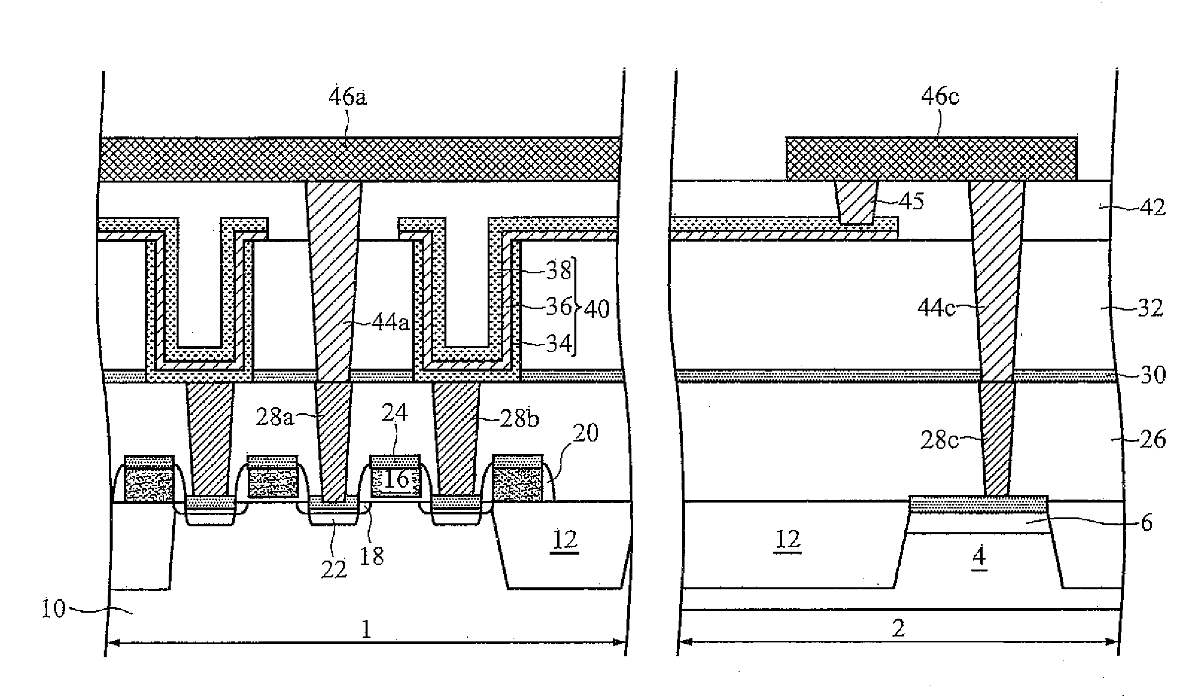
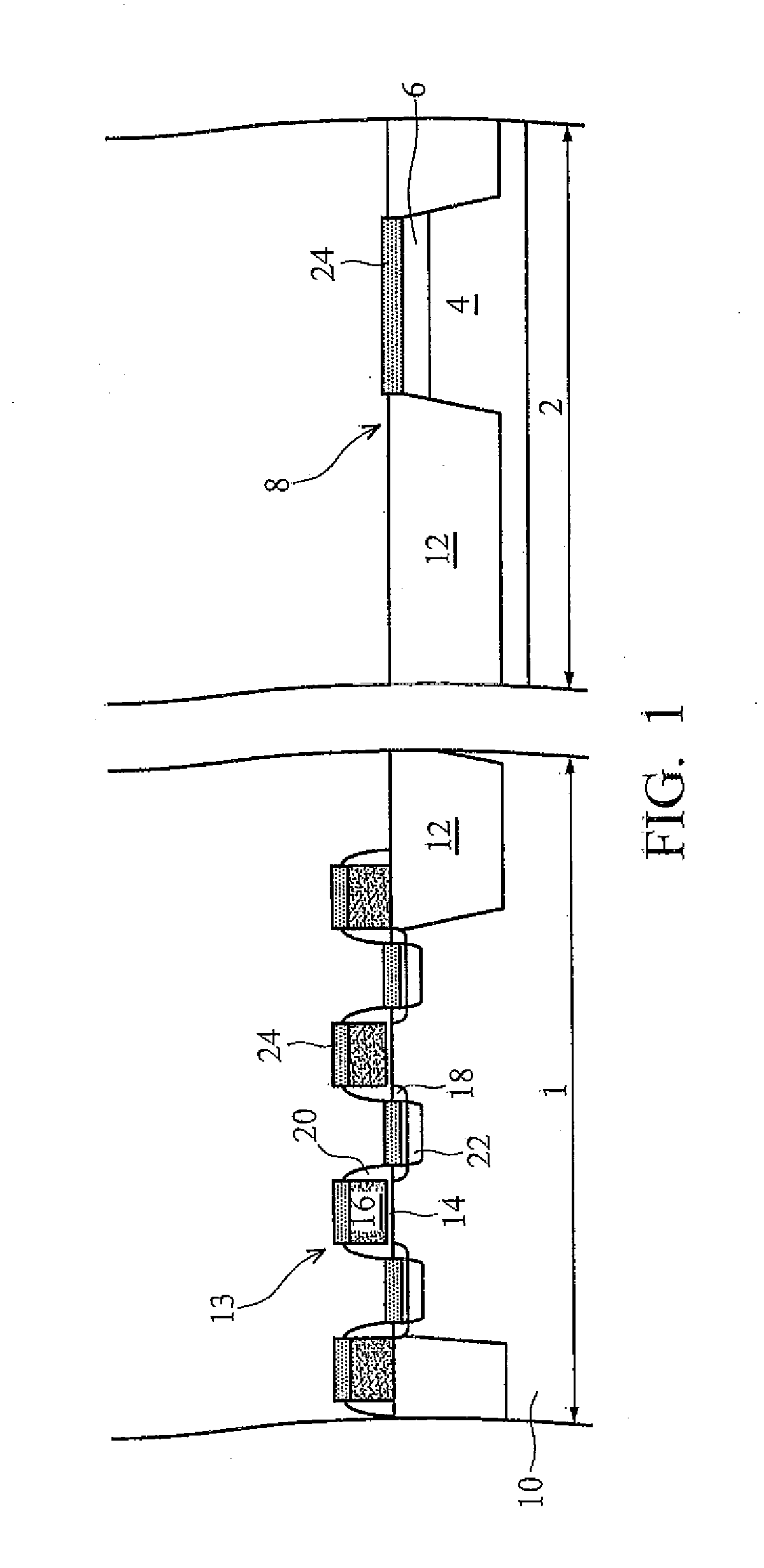
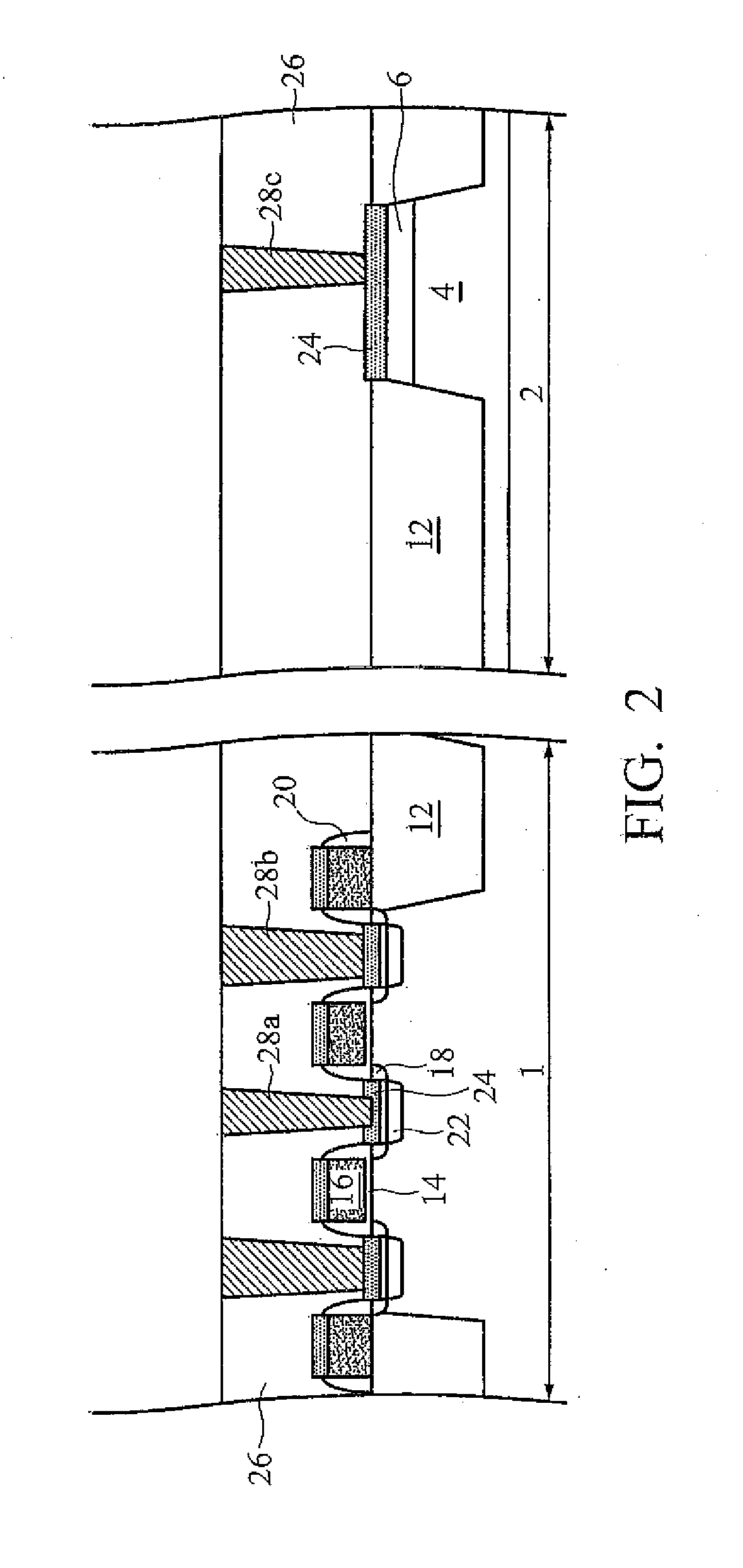
[0015]Reference will now be made in detail to the present embodiments, examples of which are illustrated in the accompanying drawings. Wherever possible, the same reference numbers are used in the drawings and the description to refer to the same or like parts. In the drawings, the shape and thickness of one embodiment may be exaggerated for clarity and convenience. This description will be directed in particular to elements forming part of, or cooperating more directly with, apparatus in accordance with the present invention. It is to be understood that elements not specifically shown or described may take various forms well known to those skilled in the art. Further, when a layer is referred to as being on another layer or “on” a substrate, it may be directly on the other layer or on the substrate, or intervening layers may also be present.

[0016]Herein, a cross-sectional diagram of FIG. 1 illustrates an exemplary embodiment of the formation of transistors 13 and a protection diode...


PUM


Abstract

A dynamic random access memory (DRAM) device has a metal-insulator-metal (MIM) capacitor electrically connected to a PN junction diode through a metal bridge for protecting the MIM capacitor from charge damage generated in back end of line (BEOL) plasma process.

Description

TECHNICAL FIELD[0001]The present invention relates to a semiconductor device, and particularly to a structure and fabrication methods for protecting a metal-insulator-metal capacitor in a memory device from charge damage.BACKGROUND[0002]In merging logic circuits and dynamic random access memory (DRAM) arrays on a single chip, compatibility is the primary issue with respect to both design and fabrication. Recently, with the continued decrease in device dimensions, it has become increasingly important to embedded DRAM technology. In semiconductor structure, DRAM capacitors have typically been either buried or stacked. Stacked capacitors can be either polycrystalline silicon (poly) or metal-insulator-metal (MIM). The MIM capacitors are embedded in the oxide layers above the active surface of the chip. Because the conductors of the interconnect layers are metal in construction, the capacitors formed between the interconnect layers are preferably of a metal-insulator-metal (MIM) construc...

Claims


Application Information

Patent Timeline
Patent Type & Authority Applications(United States)
IPC IPC(8): H01L27/108
CPCH01L27/0255H01L27/10811H01L28/60H01L27/10894H01L27/10897H01L27/10852H10B12/312H10B12/033H10B12/09H10B12/50
Inventor TU, KUO-CHICHIANG, KUO-CHENG
Owner TAIWAN SEMICON MFG CO LTD
Why Eureka
Try Eureka