Imaging assembly

a technology of assembly and assembly means, applied in the field of assembly, can solve the problems of not being able to apply anti-reflection coatings to the components of the assembly, undesirable ghost images and other stray light effects, and not being able to eliminate, so as to improve the adhesion of the spacer member, reduce stress, and improve the adhesion of the spacer means.

Active Publication Date: 2010-05-27
STMICROELECTRONICS (RES & DEV) LTD
View PDF30 Cites 74 Cited by
  • Summary
  • Abstract
  • Description
  • Claims
  • Application Information

AI Technical Summary

Benefits of technology

[0013]The substrate and / or the optical layer may be provided with surface features to aid alignment of the spacer member upon the substrate and / or the optical layer to improve adhesion of the spacer member thereto. The surface features may include a roughened surface region to improve adhesion of the spacer means to the substrate and / or the optical layer. Alternatively, the surface features may include raised formations to aid location of the spacer member on the substrate and to reduce stresses at the junction of the spacer member and the substrate and / or the optical layer.

Problems solved by technology

While such coating reduces reflections, it does not eliminate them.
A typical reflectance of such coated surfaces may be 4% or more, which will produce undesirable ghost images and other stray light effects in the image plane of such an imaging assembly.
Therefore it may not be possible to apply anti-reflection coatings to the components of the assembly, partly due to the stresses that reliable high quality (low surface defect occurrence) thin-film dielectric interference coatings place on the glass wafer.
These stresses result in deviations in flatness and warping of the glass which affects either the process of bonding the glass spacer member and package lid to the silicon wafer, or the stresses generated in the silicon as it holds the glass in tension.
This later problem results in the silicon wafer cracking as it is back-lapped (ground down to a thickness) while attached to the package lid prior to the application of the rear layer of the assembly and singulation of the glass / silicon structure to form a final chip scale package.

Method used


Image

  • Imaging assembly
  • Imaging assembly
  • Imaging assembly

Examples


Embodiment Construction

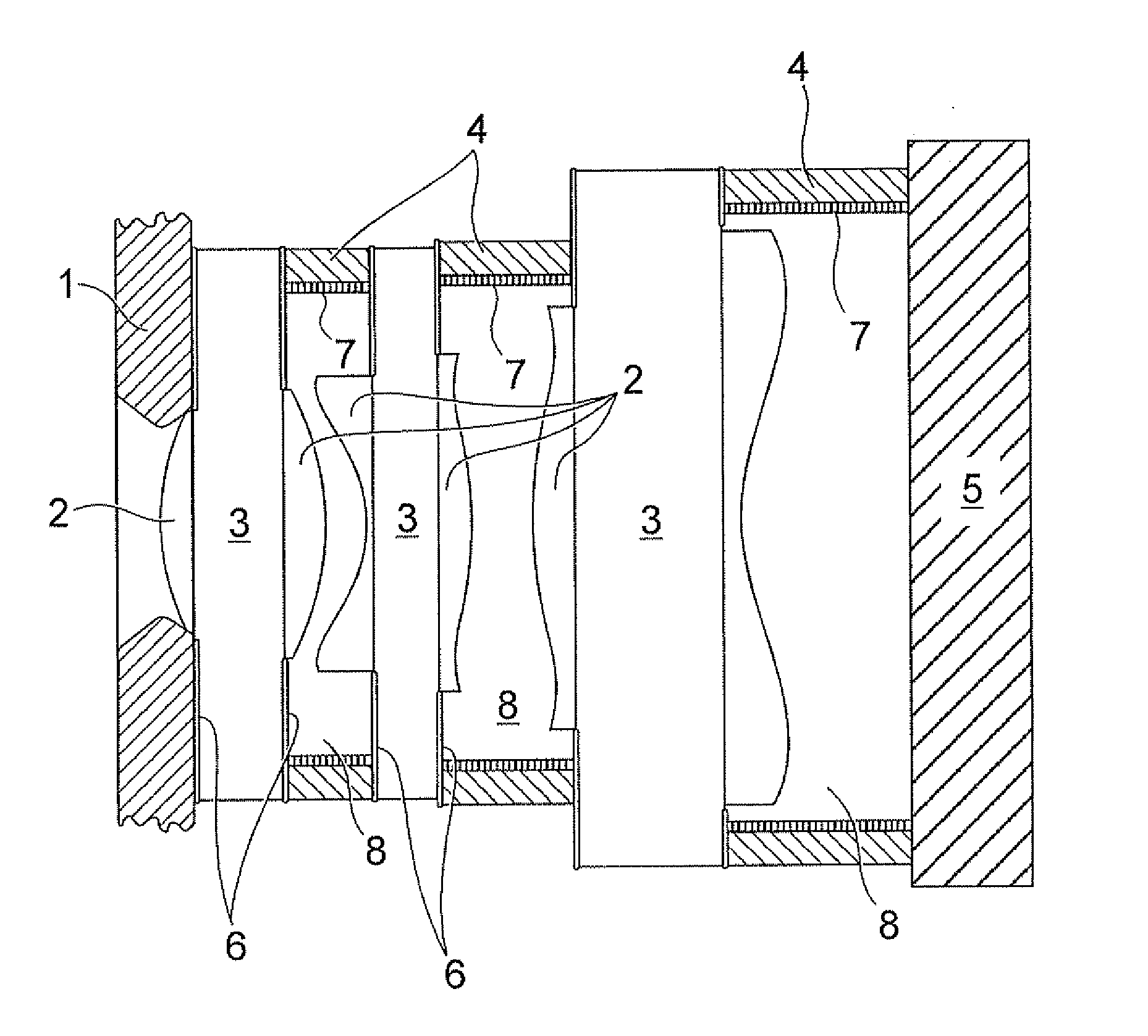
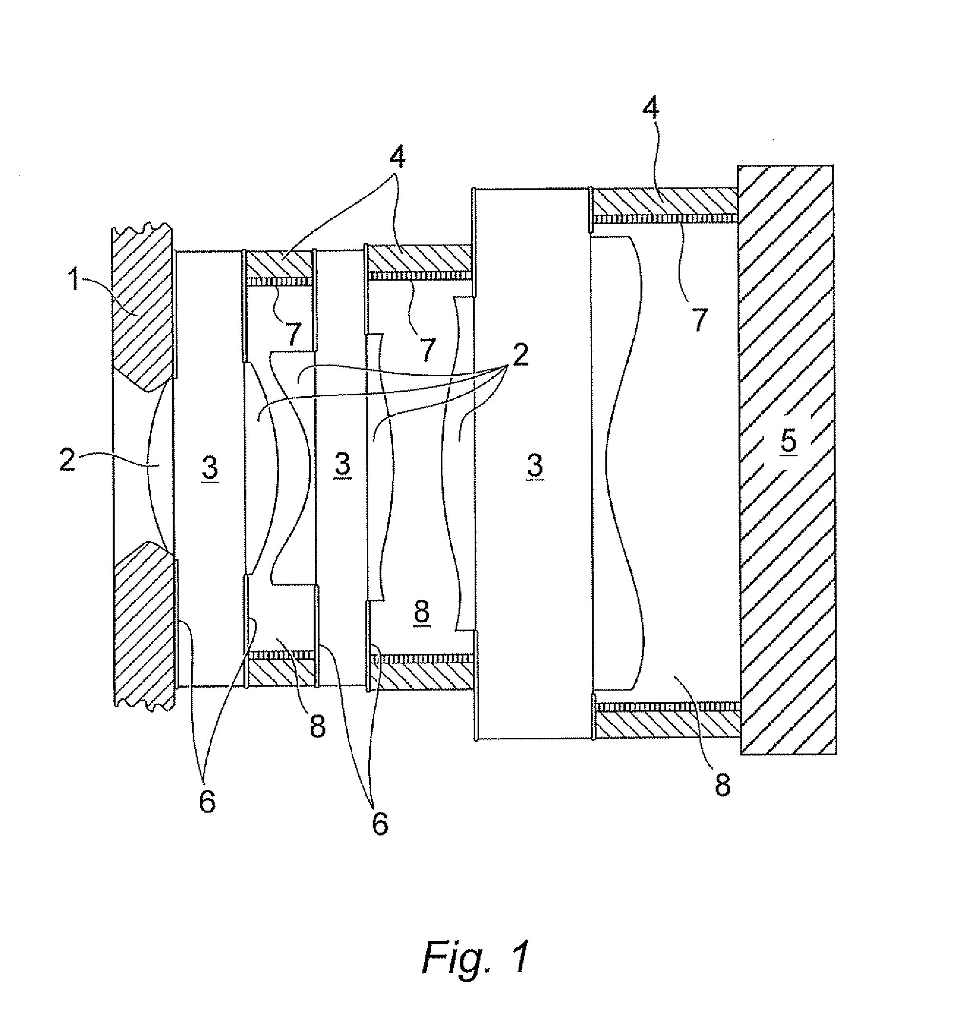
[0029]As illustrated in FIG. 1, a wafer scale lens may include a stacked arrangement of components, including, from the outermost component to the innermost, a cover 1, which provides baffling from the outside world and extends around the outermost lens element 2 to prevent light entering other than by the aperture stop, and a plurality of lens elements 2 implemented by over-molded features on substrate glass wafers 3. The lens elements 2 are separated by spacer members 4 which hold the lens elements 2 at a fixed separation from each and from an image sensor provided on a substrate 5. Air gaps 8 are therefore formed between the substrate wafers 3 and lenses 2, and within the spacer members 4.

[0030]FIG. 1 illustrates a large number of flat glass surfaces present around the lens elements 2 and also between the lens elements 2. These flat surfaces may leak and / or reflect stray-light back into the camera system, and as such, may normally require an angle of incidence insensitive absorpt...


PUM


Abstract

An image assembly may include a substrate having a face, a first optical layer and at least one spacer member. The imaging assembly may also include an anti-reflection structure. The at least one spacer member may be arranged between the substrate and the first optical layer to define an air gap therebetween. The anti-reflection structure may be coupled to at least part of the face and at least one of the first optical layer and the at least one spacer member. The anti-reflection structure may also include a plurality of projections having dimensions smaller than a wavelength of radiation to be imaged by the imaging assembly.

Description

FIELD OF THE INVENTION[0001]The present invention relates to an imaging assembly and particularly, but not exclusively, to an imaging assembly for use with solid state or wafer scale image sensors and a method of manufacturing the imaging assembly.BACKGROUND OF THE INVENTION[0002]Solid state or wafer scale image sensors are incorporated into low cost cameras and other devices, such as mobile cellular telephones and personal digital assistants, optical devices and medical imaging devices. It is known to provide wafer scale miniature cameras incorporating lenses produced using over-molding techniques on glass substrates, which can survive the high temperature solder reflow processes used in the manufacture of such devices. Such lenses are usually stacked together, separated by spacer members to provide an air gap between each lens.[0003]Currently non-light transmissive surfaces of such lens arrangements, for example, the inner faces of the spacer members, are coated with an anti-refle...

Claims


Application Information

Patent Timeline
Patent Type & Authority Applications(United States)
IPC IPC(8): G02B7/00G02B7/02H01L31/0216H01L31/18
CPCG02B1/118H01L27/14618H01L27/14632H01L27/14643H01L27/14629H01L31/02161H01L31/0232H01L2924/16235H01L2924/16788H01L27/14685H01L31/02325
Inventor FINDLAY, EWANMCGARRY, COLIN
Owner STMICROELECTRONICS (RES & DEV) LTD
Why Eureka
Try Eureka