Method, device, and program for predicting a manufacturing defect part of a semiconductor device

a technology for semiconductor devices and manufacturing defects, applied in the field of semiconductor device manufacturing defect parts, can solve the problems of increasing the design period, affecting the prediction accuracy of parts, so as to speed up the prediction of parts, and reduce the risk of manufacturing defects

Inactive Publication Date: 2010-05-27
RENESAS ELECTRONICS CORP
View PDF3 Cites 17 Cited by
  • Summary
  • Abstract
  • Description
  • Claims
  • Application Information

AI Technical Summary

Benefits of technology

[0015]In the method, the device, and the program for predicting a manufacturing defect part of a semiconductor device according to the present invention, the edge of the layout pattern of the first layout data is shifted, and the image forming position of the shifted edge on the site is calculated. Then, the error between the image forming position on the site and the edge position of the layout pattern of the first layout data is calculated, to thereby output the error information. In the method, the device, and the program for predicting a manufacturing defect part of a semiconductor device according to the present invention, based on the error information, a portion in which the image forming posit ion of the edge is unstable is predicted as a part having a high risk of a manufacturing defect. Specifically, with the method, the device, and the program for predicting a manufacturing defect part of a semiconductor device according to the present invention, it is possible to predict, without generating a contour, a part having a high risk of a manufacturing defect with simple numerical calculations.
[0016]With the method, the device, and the program for predicting a manufacturing defect part of a semiconductor device according to the present invention, it becomes possible to speed up the prediction of a part having a high risk of a manufacturing defect of a semiconductor device.

Problems solved by technology

Then, based on a result of the design rule check, a high-risk part of a manufacturing defect of a semiconductor device is predicted.
In this case, because the light intensity simulation is such arithmetic computations that require a significantly large amount of calculation, it takes a long period of time to generate a contour.
Therefore, JP 2007-536564 A, JP 2006-126745 A, JP 2008-064820 A, and JP 2008-020751 A have a problem in that an increased period of time for generating a contour results in an increase in period of time for designing.

Method used


Image

  • Method, device, and program for predicting a manufacturing defect part of a semiconductor device
  • Method, device, and program for predicting a manufacturing defect part of a semiconductor device
  • Method, device, and program for predicting a manufacturing defect part of a semiconductor device

Examples


first embodiment

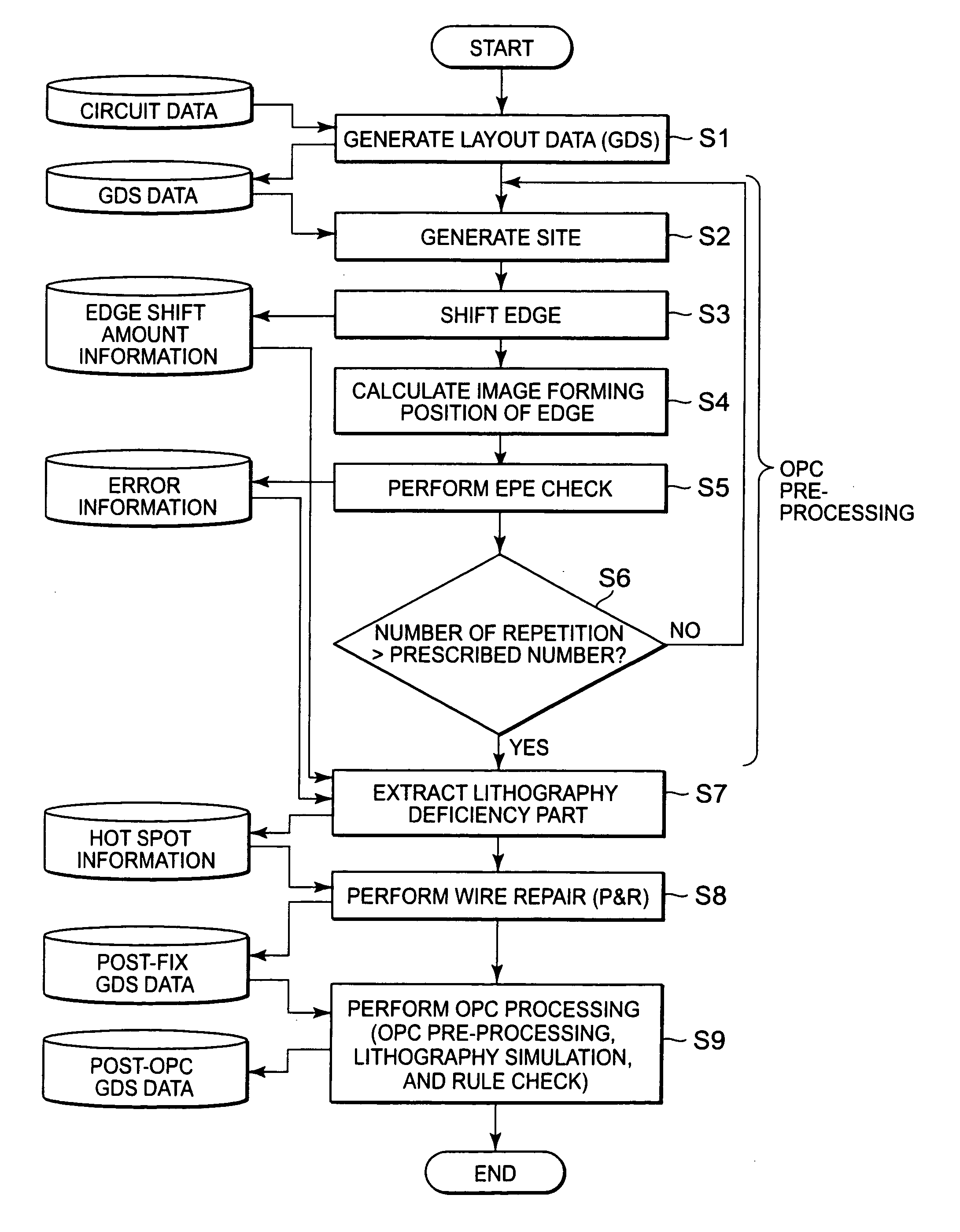
[0029]Hereinbelow, description is given of an embodiment of the present invention with reference to the attached drawings. FIG. 1 illustrates a flow chart of a method of predicting a manufacturing defect part of a semiconductor device according to this embodiment. Of a semiconductor design process according to this embodiment, the flow chart of FIG. 1 illustrates a flow of optical proximity correction (OPC) processing performed on layout data. In this embodiment, before the flow chart illustrated in FIG. 1 is started, a circuit design process is performed, and after the flow chart illustrated in FIG. 1 is finished, reticle manufacturing and semiconductor manufacturing process are further performed. Incidentally, the prediction of a manufacturing defect part of a semiconductor device according to this embodiment is performed as one processing step included in the OPC processing. However, the prediction of a manufacturing defect part may be performed as processing independent of the r...


PUM

PropertyMeasurementUnit
optical proximity correctionaaaaaaaaaa
manufacturing defectaaaaaaaaaa
light intensity simulationaaaaaaaaaa

Abstract

Provided is a method of predicting a manufacturing defect part of a semiconductor device, which results from optical pattern displacement in an exposure process. The prediction method includes: performing repetitive processing a plurality of times, the repetitive processing including: a site generating step of setting a site at a predetermined position of a layout pattern; an edge shifting step of shifting an edge of the layout pattern according to a predetermined rule; an image forming position calculating step of calculating an image forming position corresponding to the shifted edge on the site; and an error check step of storing error information between the image forming position on the site and the edge of the layout pattern; and extracting, based on the error information, from the first layout data, apart in which the image forming position is unstable, and predicting the extracted part as a hot spot.

Description

BACKGROUND OF THE INVENTION[0001]1. Field of the Invention[0002]The present invention relates to a method, device, and program for predicting a manufacturing defect part of a semiconductor device, which are used in optical proximity correction (OPC) processing in which optical proximity correction is performed on a circuit pattern to be formed on a semiconductor substrate.[0003]2. Description of the Related Art[0004]In recent years, a manufacturing process for a semiconductor has been proceeding toward finer patterning. Along with this trend toward finer patterning, in an exposure process of the manufacturing process for a semiconductor, displacement between a reticle pattern and a circuit pattern actually formed on a semiconductor substrate has becoming increasingly conspicuous due to an optical proximity effect. Here, the reticle pattern refers to an exposure mask, which has a pattern based on image data (hereinafter, referred to as GDS data) of a circuit pattern generated in a la...

Claims


Application Information

Patent Timeline
Patent Type & Authority Applications(United States)
IPC IPC(8): G06F17/50G03F1/36G03F1/68H01L21/027
CPCG03F1/144G06F17/5081G03F1/36G06F30/398
Inventor HIRABAYASHI, KEISUKE
Owner RENESAS ELECTRONICS CORP
Why Eureka
Try Eureka