Three-dimensional architecture for integration of CMOS circuits and nano-material in hybrid digital circuits

a technology of cmos circuits and nano-materials, applied in the field of three-dimensional architecture for integrating cmos circuits with nano-materials, can solve the problems of less likely use of misalignment, and achieve the effect of convenient connection of nanowires and efficient utilization of nanowire densities

Inactive Publication Date: 2010-06-03
THE RES FOUND OF STATE UNIV OF NEW YORK
View PDF3 Cites 12 Cited by
  • Summary
  • Abstract
  • Description
  • Claims
  • Application Information

AI Technical Summary

Benefits of technology

[0005]A structure enabling more efficient utilization of the nanowire densities possible in CMOL is desirable. Additionally, a structu...

Problems solved by technology

Additionally, a structure that facilitates the connection of the nanowires to ...

Method used


Image

  • Three-dimensional architecture for integration of CMOS circuits and nano-material in hybrid digital circuits
  • Three-dimensional architecture for integration of CMOS circuits and nano-material in hybrid digital circuits
  • Three-dimensional architecture for integration of CMOS circuits and nano-material in hybrid digital circuits

Examples


Embodiment Construction

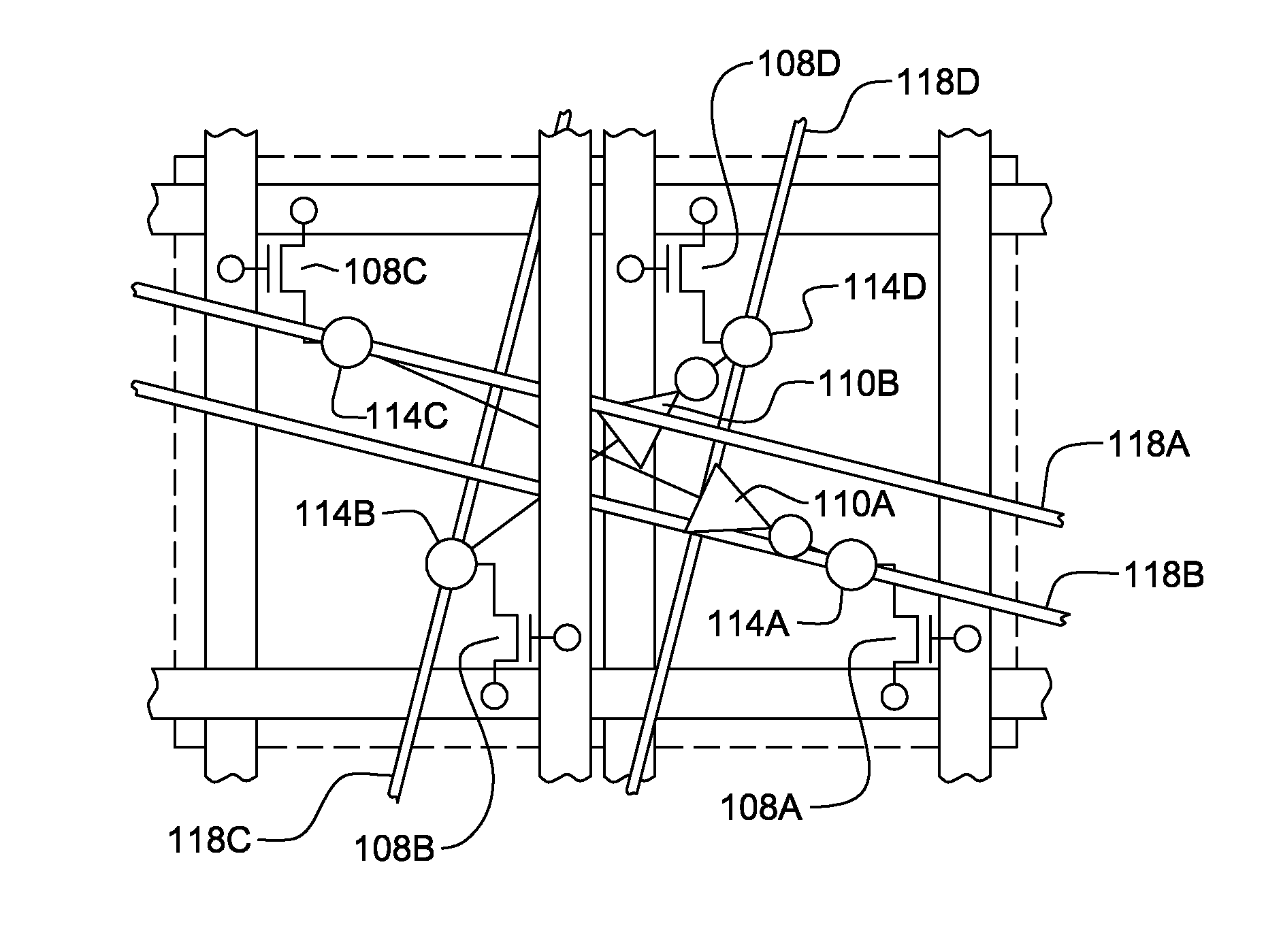
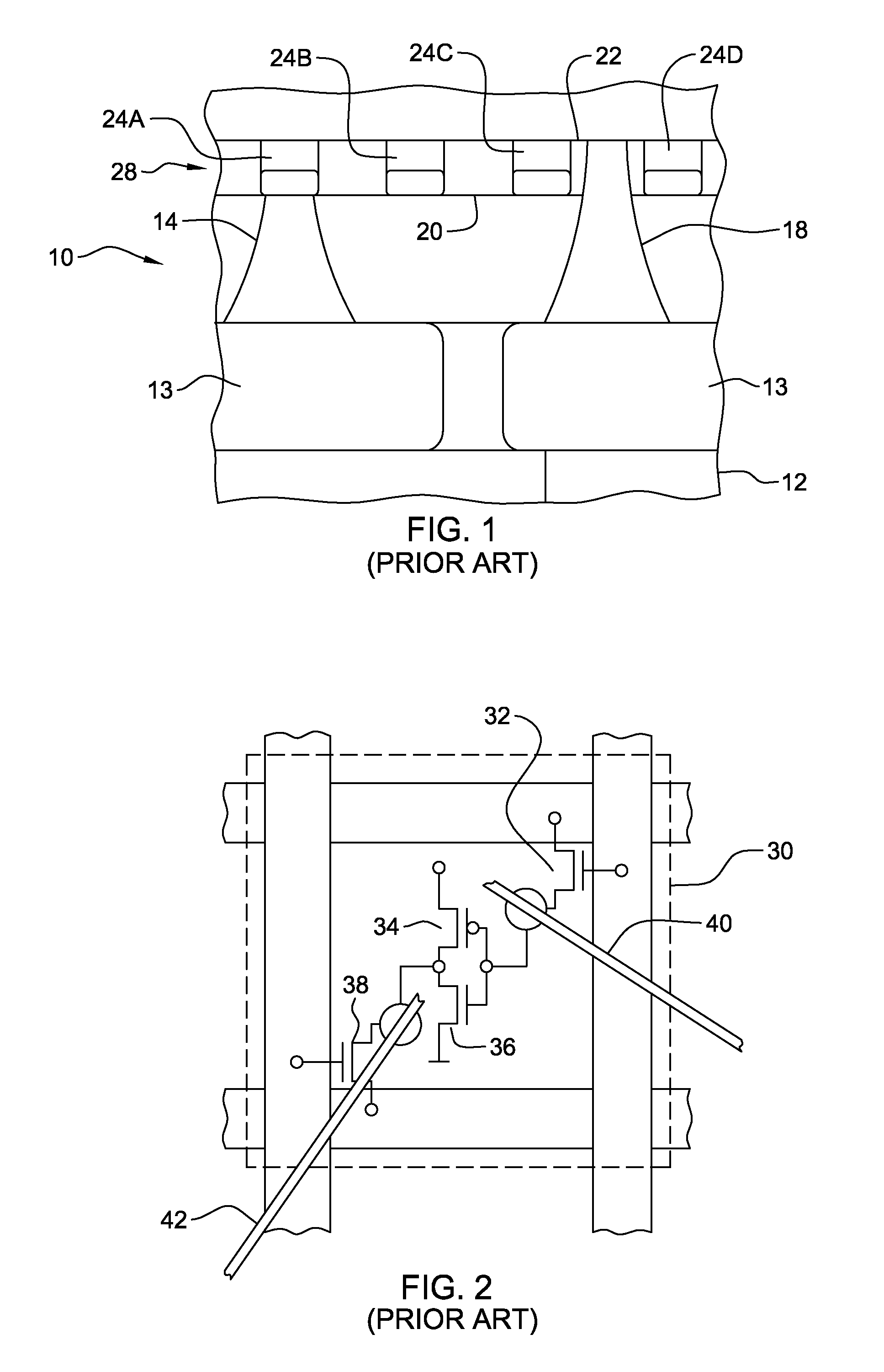
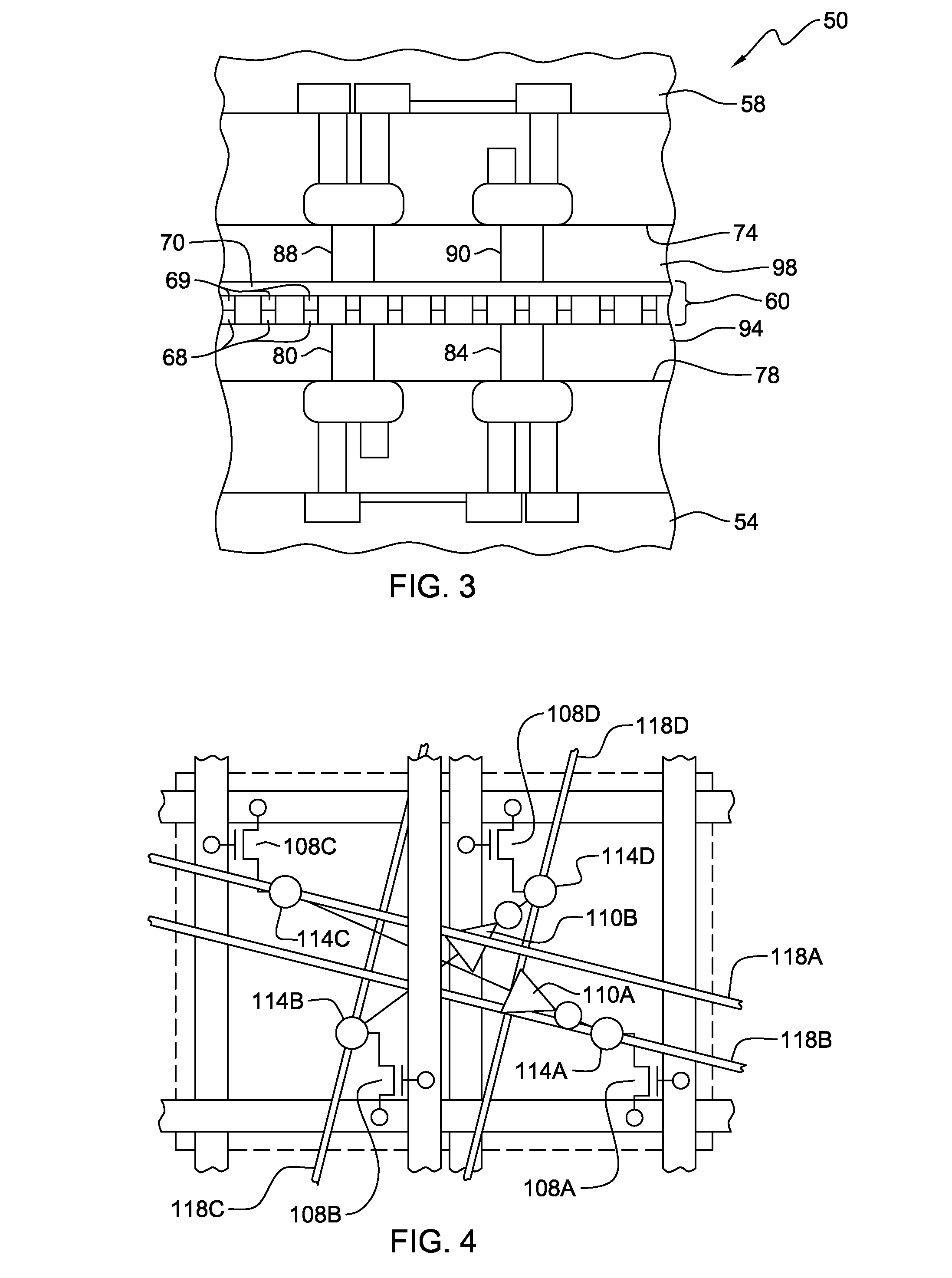
[0019]As shown in FIG. 3, a three dimensional (3D) CMOL structure is depicted that overcomes the limitations of previously known CMOL structures. The 3D CMOL structure 50 includes two face-to-face stacks of CMOS circuits 54, 58 and nanowire crossbar switches 60 in an intervening layer. “Face-to-face” means that the CMOS structures are oriented in the stack so the CMOS device layers formed on the respective substrates face one another. Bottom and top arrays of nanowires 68, 70 in the nanowire crossbar switch layer 60 are connected to the bottom 74 and top 78 of the CMOS structures, respectfully, by separated interface pins 80, 84, 88, and 90. Interface pins 80, 84 are within a first interconnect layer 94 and interface pins 88, 90 are within a second interconnect layer 98. The interface pins may be metal or any other suitable conductive material, including superconductive materials. This structure enables the CMOS cells to be coupled to the nanowire crossbar switches 60 in a manner th...


PUM


Abstract

A hybrid CMOL stack enables more efficient design of CMOS logical circuits. The hybrid CMOL structure includes a first substrate having a CMOS device layer on the substrate, a first interconnect layer with interface pins over the CMOS device layer of the first substrate, a first array of nanowires connected to the interface pins of the first interconnect layer, a layer of nanowire junction material over the first array of nanowires, a second array of nanowires over the nanowire junction material, a second interconnect layer having interface pins disposed over the second array of nanowires, the interface pins being connected to the second array of nanowires, and a second substrate, the second substrate including a second CMOS device layer disposed over the second interconnect layer.

Description

TECHNICAL FIELD[0001]The present invention relates generally to complementary metal oxide semiconductor (CMOS) circuit architecture and, in particular, to the integration of CMOS circuits with nano-material.BACKGROUND OF THE INVENTION[0002]The use of nano-materials with electronic circuit devices to establish field programmable gate array (FPGA) type structures has resulted in different device fabrication methods. One particular method is a cell-based architecture called hybrid nanowire / molecular / semiconductor circuit, which is sometimes referred to as ‘CMOL.’ In this structure, high-density nanowire crossbars and molecular (nanowire junction or bistable junction) switches are fabricated on top of a CMOS stack to build a number of basic logical circuit cells in a logic memory arrangement. This technique is promoted as showing advantages over standard CMOS FPGA structure, such as device density and fault tolerance capabilities.[0003]One key technique used in CMOL is an interface sche...

Claims


Application Information

Patent Timeline
IPC IPC(8): H01L27/092H01L21/8234
CPCB82Y10/00G11C13/0007H01L27/101G11C2213/71G11C2213/81G11C2213/34Y10S977/762
Inventor WANG, WEI
Owner THE RES FOUND OF STATE UNIV OF NEW YORK
Why Eureka
Try Eureka