Screening of Silicon Wafers Used in Photovoltaics

a technology of photovoltaics and silicon wafers, applied in the field of semiconductor/solid-state device testing/measurement, force measurement by measuring optical property variation, instruments, etc., can solve the problems of reducing the yield to unacceptable values, adding significant costs, and difficult manufacturing implementation

Inactive Publication Date: 2010-06-03
ALLIANCE FOR SUSTAINABLE ENERGY
View PDF21 Cites 17 Cited by
  • Summary
  • Abstract
  • Description
  • Claims
  • Application Information

AI Technical Summary

Problems solved by technology

Although the concept of reducing wafer thickness is quite straightforward, it is difficult to implement in manufacturing.
Additional reductions in the wafer thickness are found to further decrease the yield to unacceptable values.
These preventive measures add significant costs.
The photovoltaic industry finds that it is not able to adopt these preventive measures due to the high cost that is associated with these procedures.
Thus, the excessive breakage of wafers in the photovoltaic industry is primarily due to inadequate wafer preparation, inexpensive wafer handling, and low-cost device processing methods, which are all aimed at minimizing the cost of the solar cell.
This incomplete wafer preparation in the photovoltaic industry leaves such as microcracks at the surfaces and the edges of the wafers, which lead to wafer breakage during cell fabrication as discussed later.
Typical defects are metal film peeling from insulating dielectric material layer or void formation.
These techniques are difficult to use on photovoltaic wafers for detection of flaws and defects because these wafers have rough surfaces.
The surface roughness “hides” such flaws and microcracks, making it difficult to recognize their presence by optical techniques.
Other limitations of the related art will become apparent to those of skill in the art upon a reading of the specification and a study of the drawings.

Method used


Image

  • Screening of Silicon Wafers Used in Photovoltaics
  • Screening of Silicon Wafers Used in Photovoltaics
  • Screening of Silicon Wafers Used in Photovoltaics

Examples


example 1

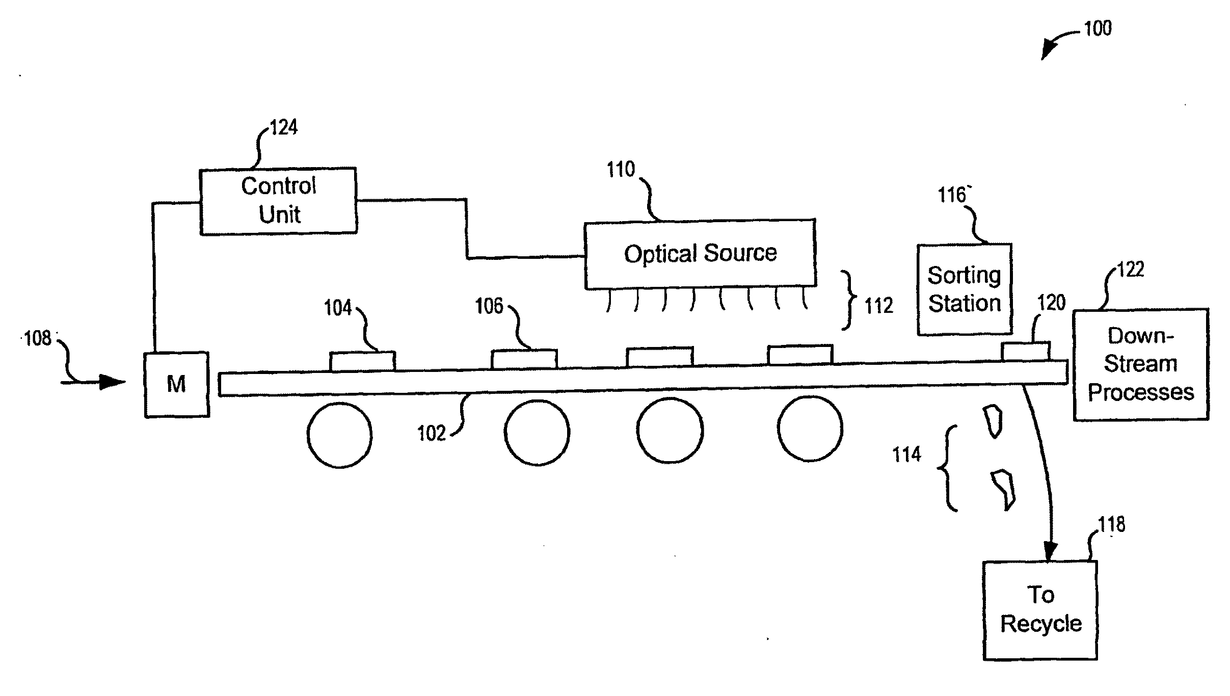
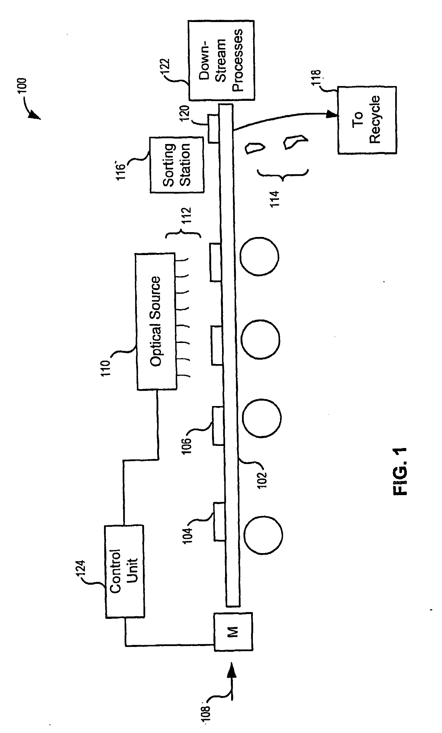
[0076]The practical implementation of the above principles may easily be performed in a system consisting of a light source and a conveyor belt arrangement as shown in FIG. 8, which shows a schematic of a simple setup for isolating wafers likely to break during solar cell processing. Since the embodiment shown in FIG. 8 is representative of the system 100 shown in FIG. 1, like numbering of identical parts is designated by a “′”, such as system 100′ of FIG. 8.

[0077]The wafers are sequentially placed on a belt, which preferably supports the wafers at the edges. They are conveyed into a region which has a narrow illuminated zone. As the wafers pass under this illumination, each wafer acquires a temperature-distribution, which depends on the intensity pattern of the light, the size of the wafer, and the belt speed. This results in a predetermined thermal stress.

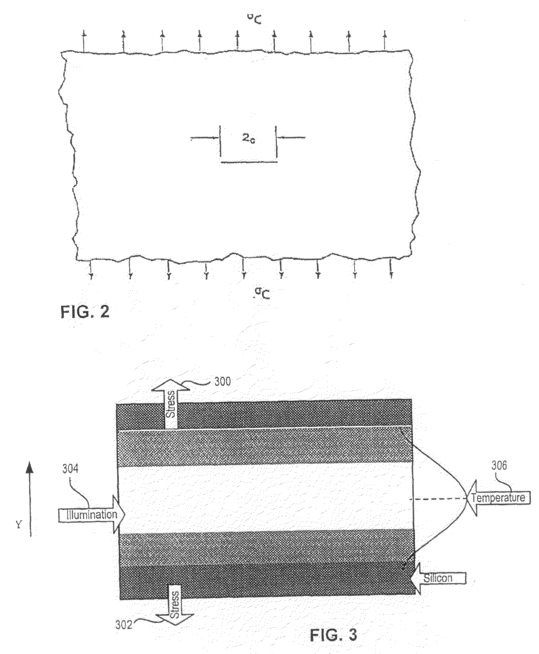
[0078]As a result of non-uniform heating, a stress distribution is induced in the wafer. The illumination pattern is chosen to ...


PUM

PropertyMeasurementUnit
thicknessaaaaaaaaaa
defect sizeaaaaaaaaaa
temperatureaaaaaaaaaa

Abstract

A method for screening silicon-based wafers used in the photovoltaic industry is provided herewith.

Description

CONTRACTUAL ORIGIN OF THE INVENTION [0001]The United States Government has rights in this invention under Contract No. DE-AC36-99G010337 between the United States Department of Energy and the National Renewable Energy Laboratory, a Division of the Midwest Research Institute.BACKGROUND ART [0002]The present disclosure relates to semiconductor wafers, such as silicon wafers that are used as substrates for making photovoltaic devices.[0003]One of the strategies for lowering the cost of silicon-based photovoltaic (PV) energy is to use thinner wafers for solar cell fabrication. This strategy reduces the wafer cost and increases solar cell efficiency, provided appropriate cell design and processing techniques are employed. Although the concept of reducing wafer thickness is quite straightforward, it is difficult to implement in manufacturing. The experience in the industry is that even for the current wafers, which have a nominal thickness of about 250 μm, the breakage during solar cell f...

Claims


Application Information

Patent Timeline
Patent Type & Authority Applications(United States)
IPC IPC(8): H01L31/18G01N3/60H01L21/66
CPCG01N21/9503H01L31/18G01N21/9505
Inventor SOPORI, BHUSHAN L.SHELDON, PETER
Owner ALLIANCE FOR SUSTAINABLE ENERGY
Why Eureka
Try Eureka