Solar cell with high conversion efficiency

A solar cell, high-conversion technology, applied in circuits, electrical components, photovoltaic power generation, etc., can solve problems such as process incompatibility, and achieve the effects of improving conversion efficiency, improving light absorption, and enhancing light absorption

Inactive Publication Date: 2011-06-15
CHONGQING UNIV
View PDF6 Cites 16 Cited by
  • Summary
  • Abstract
  • Description
  • Claims
  • Application Information

AI Technical Summary

Problems solved by technology

[0003] The purpose of the present invention is to propose a method of using periodic nanostructures to make the anti-reflection film on the surface of solar cells into nanostructures to improve the conversion efficiency of solar cells, and the nanostructures can be processed by photolithography and etching techniques to solve and present problems. There are process incompatibility issues

Method used


Image

  • Solar cell with high conversion efficiency
  • Solar cell with high conversion efficiency
  • Solar cell with high conversion efficiency

Examples


Embodiment Construction

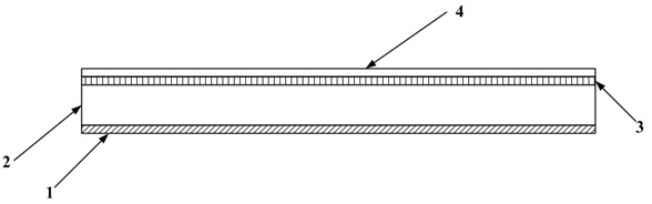
[0021] figure 1 Shown is a solar cell structure, the basic material of which is a P-type monocrystalline silicon wafer, the upper surface of which is an N+-type region to form a PN+ junction 2, and a grid-like metal electrode 3 is formed on the upper surface of the PN+ junction 2, and the grid-like metal electrode The surface of 3 is evenly covered with an anti-reflection film 4, and a metal bottom electrode 1 is formed on the lower surface of the P-type single crystal silicon wafer.

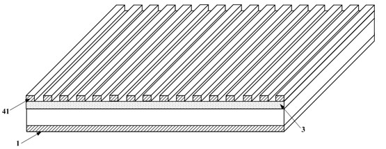
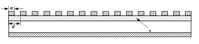
[0022] Such as figure 2 , Figure 2.a As shown, periodic nano-gratings 41 are formed in the anti-reflection coating 4, and the nano-gratings 41 are processed in the anti-reflection coating 4, and the porosity P= a / d (consistent with the duty cycle of the grating), by changing the period d and the duty cycle can change the porosity of the grating. According to formula (1), the equivalent refractive index of the anti-reflection coating is also changed, so that the equivalent refractive ind...


PUM

PropertyMeasurementUnit
lattice constantaaaaaaaaaa

Abstract

The invention discloses a solar cell with high conversion efficiency, which belongs to the field of semiconductor material application. The solar cell is formed by forming a periodical nanostructure such as a nano wire grating and a nanopore array in a conventional antireflection coating of the solar cell. The nanostructure can reduce an effective refractive index of the antireflection coating, and makes a refractive index of the antireflection coating matched with a substrate so as to improve the reflection resistance of the coating and enhance the light absorption of the solar cell to further improve the conversion efficiency of the solar cell. Theoretical analysis shows that the conversion efficiency of the solar cell adopting the antireflection coating with the nanostructure is relatively more improved at 400 to 1,000 nm, and particularly is greatly improved at short-wave bands. The nanostructure can be realized only by using photoetching and etching based on a conventional solar cell processing technique, and the processing technique is compatible with the conventional solar cell processing technique, and can be widely applied to the photovoltaic industry.

Description

technical field [0001] The invention relates to a technology for improving the conversion efficiency of solar energy, in particular to an antireflection film solar cell with a periodic nanostructure, which belongs to the application field of semiconductor materials. Background technique [0002] Due to the advantages of low cost, abundant storage, non-toxicity, stability and mature processing technology, silicon material is the best choice for making photovoltaic devices. Current commercial photovoltaic devices usually have 200-300 mm The active layer of silicon, which accounts for about 40% of the cost of photovoltaic devices, is very expensive for a wide range of applications. In order to reduce the cost of a wide range of applications, researchers have proposed thin-film solar cells with only a few microns of silicon active layer, but the thinner the active layer, the weaker the light absorption of photovoltaic devices, resulting in a reduction in the conversion efficien...

Claims


Application Information

Patent Timeline
Patent Type & Authority Applications(China)
IPC IPC(8): H01L31/0216H01L31/0224H01L31/04H01L31/0232
CPCY02E10/50
Inventor 朱永王宁陈建君韦玮李平文玉梅
Owner CHONGQING UNIV
Why Eureka
Try Eureka