Slow-Wave Coaxial Transmission Line Formed Using CMOS Processes

Active Publication Date: 2010-06-10
TAIWAN SEMICON MFG CO LTD
21 Cites 43 Cited by

AI-Extracted Technical Summary

Problems solved by technology

However, the formation of ground plane 8 also incurs drawbacks.
Consequently, Ohmic losses in microstrip lines become increasingly more significant, thus demanding better impedance matching between microstrip line 2 and other network devices.
In addition, microstrip lines typically occup...

Benefits of technology

[0011]The advantageous features of the present invention include reduced energy loss in coaxial transmission lines, and tunable characterist...

Abstract

An integrated circuit structure includes an interconnect structure over a semiconductor substrate and a coaxial transmission line. The coaxial transmission line includes a signal line, a top plate over the signal line and electrically insulated from the signal line, and a bottom plate under the signal line and electrically insulated from the signal line. At least one of the top plate and the bottom plate includes metal strip shields and dielectric strips, with each of the dielectric strips being between two of the metal strip shields. The integrated circuit structure further includes a ground conductor electrically connecting the top plate and the bottom plate. The ground conductor is insulated from the signal line by a dielectric material.

Application Domain

Technology Topic

Image

  • Slow-Wave Coaxial Transmission Line Formed Using CMOS Processes
  • Slow-Wave Coaxial Transmission Line Formed Using CMOS Processes
  • Slow-Wave Coaxial Transmission Line Formed Using CMOS Processes

Examples

  • Experimental program(1)

Example

[0022]The making and using of the presently preferred embodiments are discussed in detail below. It should be appreciated, however, that the present invention provides many applicable inventive concepts that can be embodied in a wide variety of specific contexts. The specific embodiments discussed are merely illustrative of specific ways to make and use the invention, and do not limit the scope of the invention.
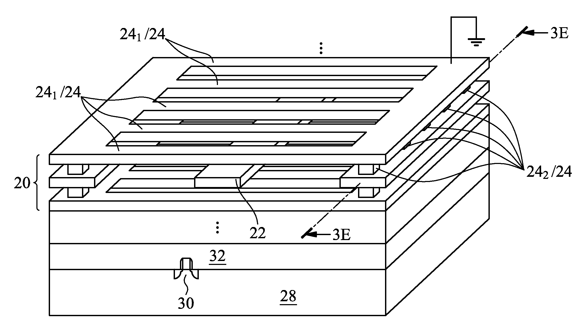
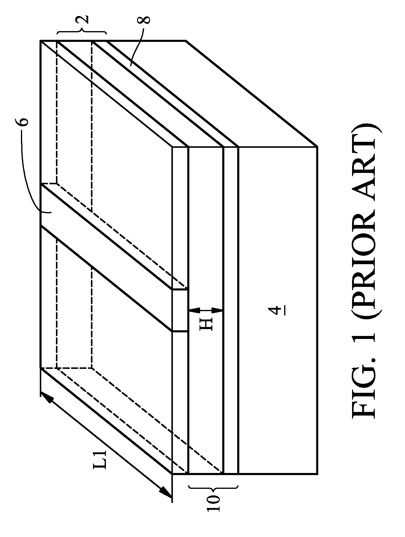
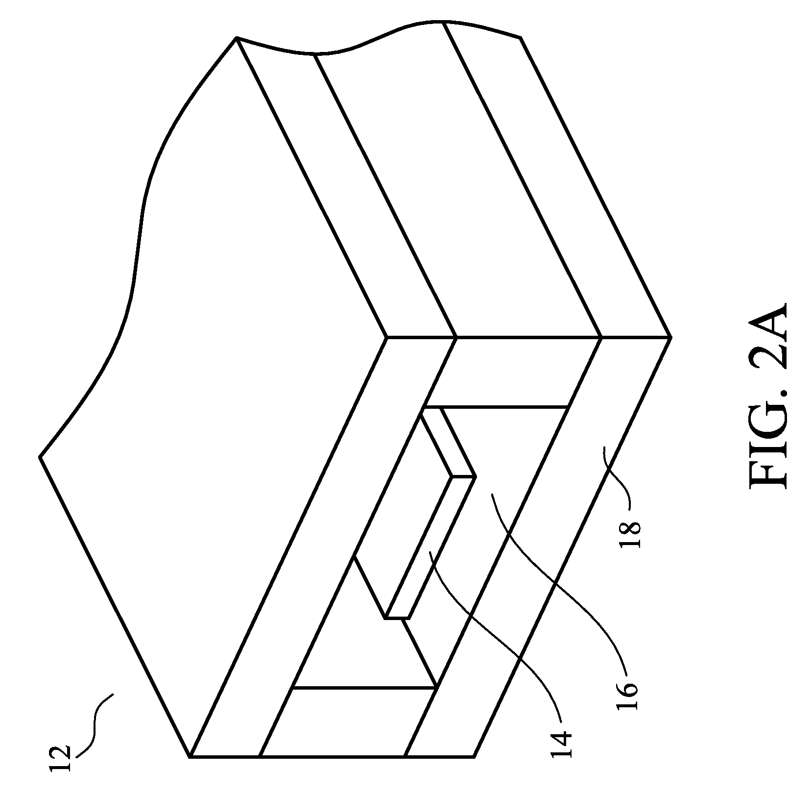
[0023]Since conventional unshielded transmission lines suffer from high-energy loss, coaxial transmission lines were developed for more efficient signal transmission. U.S. patent application Ser. No. 12/023,184, which is incorporated herein by reference, discloses coaxial transmission line 12, as shown in FIGS. 2A and 2B. FIG. 2A is a perspective view, while FIG. 2B is a cross-sectional view, of coaxial transmission line 12. Signal line 14 is surrounded by dielectric material(s) 16. Encircling dielectric material(s) 16 is ground line 18, which forms a solid metal shield for signal line 14. Since signal line 14 is surrounded by ground line 18, the leakage of electromagnetic fields, if any, is minimal, and hence the energy loss is minimized.
[0024]The manufacturing of coaxial transmission line 12, however, faces process difficulties. Since the length and the width of coaxial transmission line 12 typically have great values, the manufacturing process violates the CMOS design rules. Particularly, the manufacturing of coaxial transmission line 12 involves chemical mechanical polishes (CMPs). However, the great size of the top plate and the bottom plate of ground line 18 causes the well-known micro-loading effect and dishing effect. In addition, the propagation speed of coaxial transmission line 12 is controlled only by the properties of dielectric material 16, and thus it is difficult to tune the characteristic wavelength of coaxial transmission line 12.
[0025]To improve the process compatibility of coaxial transmission lines with the CMOS manufacturing processes and to make the characteristic wavelengths adjustable, novel coaxial transmission lines having tunable characteristic impedances and tunable characteristic wavelengths are provided. The variations of the preferred embodiments are then discussed. Throughout the various views and illustrative embodiments of the present invention, like reference numbers are used to designate like elements.
[0026]Embodiments of the invention relate to integrated circuits having a coaxial transmission line including at least one ground conductor coupled with a top plate and a bottom plate, at least one of which having metal strip shields and dielectric strips, each dielectric strip between two of the metal strip shields. The coaxial transmission line can provide tunable characteristic impedances and/or slow-wave features by adjusting widths and spacings of the metal strip shields.
[0027]FIG. 3A illustrates a perspective view of an exemplary embodiment. Coaxial transmission line 20, which includes signal line 22, patterned ground line 24, and dielectric layer(s) 26 (refer to FIG. 3B), is formed over substrate 28. In an embodiment, substrate 28 is a semiconductor substrate, and may include commonly used semiconductor materials such as silicon, germanium, and the like. The structure shown in FIG. 3A is a portion of a semiconductor chip, which may further include other regions having no microwave transmission line(s) formed thereon. Integrated circuits 30, such as complementary metal-oxide-semiconductor (CMOS) devices, may be formed at the surface of substrate 28. Integrated circuits 30 are symbolized by a MOS device.
[0028]FIG. 3B illustrates a cross-sectional view of the structure shown in FIG. 3A, wherein the cross-sectional view is taken along a vertical plane crossing line 3B-3B in FIG. 3A. Ground line 24, as the name suggests, is preferably grounded. Ground line 24 may be formed over inter-layer dielectric (ILD) 32, in which contact plugs (not shown) connected to the integrated circuits 30 are formed. In an embodiment, ground line 24 extends through a plurality metallization layers, which may include one or more metallization layers (including any of the layers ranging from bottom metallization layer (also well known as metallization layer M1) to top metallization layer (Mtop)). Dielectric layers 26 may thus include low-k dielectric materials, for example, with dielectric constants lower than about 3.0, or even about 2.5 or lower. Ground line 24 may also extend into upper dielectric layers including an un-doped silicate glass (USG) layer and even the overlying passivation layers that are commonly formed using non-dual damascene processes.
[0029]Referring to FIGS. 3A and 3B, ground line 24, which is formed of metals, for example, copper, includes a top plate overlying signal line 22, and a bottom plate underlying signal line 22. In the preferred embodiment, both the top plate and the bottom plate include a plurality of metal strip shields 241 separated from each other and having lengthwise directions perpendicular to the lengthwise direction of signal line 22. Preferably, the angle a as shown in FIG. 3C is 90 degrees, although angle a may be smaller or greater than 90 degrees. In alternative embodiments, only one of the top plate and the bottom plate includes metal strip shields 241 separated by dielectric materials, while the other one form a solid plate. Ground conductors 242, which are the sidewall portions of ground line 24, interconnect metal strip shields 241. In the preferred embodiment, ground conductors 242 are parallel to, or are at least substantially parallel to, signal line 22. Each of the metal strip shields 241 in the top plate preferably vertically overlaps one of the metal strip shields 241 in the bottom plate, although they may also be vertically misaligned.
[0030]Referring to FIG. 3C, which is a top view of the structure shown in FIG. 3A (the top plate is not shown), metal strip shields 241 have lengths SL, and are spaced from each other by dielectric regions 36 (alternatively referred to as dielectric strips hereinafter), whose widths are also the spacings SS between metal strip shields 241. To effectively shield substrate 28 from the signal carried in signal line 22 and considering the transmission line performance, such as attenuation loss, quality factor, and wavelength, lengths SL can be as small as possible. In embodiments, lengths SL can be less than about twice the minimum lengths allowed by the forming technology. In other embodiments, lengths SL can be equal to the minimum length. In an exemplary embodiment in which the integrated circuits are formed using 45 nm technology, lengths SL and strip spacings SS can be between about 70 nm and about 4 μm. The design for various combinations of different strip lengths SL and strip spacings SS is considered based on the specification requirement for different applications. The values of spacing SS and lengths SL of strip shields 241 may affect the performance of the characteristic impedance and the characteristic wavelength of the resulting coaxial transmission line 20, and the optimum values can be found through experiments. In the preferred embodiment, signal line 22 is located horizontally in the middle of the opposing ground conductors 242, and is spaced apart from ground conductors 242 by spacing S.
[0031]Strip lengths SL of different strip shields 241 preferably have a periodic pattern, that is, neighboring strip shields 241 may be grouped, with strip lengths SL of strip shields 241 in one group repeating the width pattern in other groups. In each of the groups, the strip lengths SL may be arranged in an order from smaller to greater (for example, forming an arithmetic sequence or a geometric sequence), with each of strip lengths SL being greater than a previous one. More preferably, in each of the top plate and the bottom plate of ground line 24, all of strip shields 241 preferably have a same strip length SL, although strip lengths SL may also be different from each other. Similarly, all spacings SS between neighboring strip shields 241 are preferably equal to each other. Alternatively, spacings SS may have other periodic patterns similar to that of strip lengths SL.
[0032]The formation methods of signal line 22 and ground line 24 may include commonly known single and dual damascene processes, wherein signal line 22 and ground line 24 are formed of copper or copper alloys. Accordingly, signal line 22 may include only a metal line portion, but not a via portion. Alternatively, as shown in FIG. 3B, signal line 22 may include a metal line portion 22M and an underlying via portion 22V. Further, signal line 22 may span into more than one dielectric layer, with one metal line portion and one via portion of signal line 22 in each of the dielectric layers. In the case signal line 22 and/or ground line 24 extend into the passivation layers, the formation methods may include depositing a metal layer, patterning the metal layer by etching, and filling the spacing between the remaining portions of the metal layer with dielectric materials.
[0033]Referring to FIGS. 3D and 3E, ground line 24 includes a plurality of portions, each located in one of dielectric layers 26. In an embodiment of the present invention, the portions of ground line 24 in different dielectric layers 26 are interconnected by via bars 242 — V that are co-terminus with the overlying metal line portion 242 — M. Accordingly, as shown in FIG. 3D (a cross-sectional view taken along a vertical plane crossing line 3D-3D in FIG. 3A), ground conductors 242 are solid sidewalls. Alternatively, in FIG. 3E, which is an alternative cross-sectional view taken along the vertical plane crossing line 3E-3E in FIG. 4 (an alternative embodiment of the present invention), the via portions of ground conductors 242 include periodically located via columns underlying metal lines portions, wherein the metal line portions are continuous. The via portions of ground conductors 242 are separated from each other by dielectric regions. Similarly, signal line 22 may also include more than one layer, each located in a metallization layer, with via columns or solid via bars connecting the layers of signal line 22.
[0034]In coaxial transmission lines that have solid ground planes, the signal return path is mostly in the top plate and the bottom plate, and at positions directly overlying and underlying the respective signal line. Advantageously, in the embodiments of the present invention, dielectric strips 36 (refer to FIG. 3C) traverse the signal return path directly overlying and underlying signal line 22. The signal return paths are thus forced to ground conductors 242, which are spaced far from signal line 22. Accordingly, the characteristic impedance and characteristic wavelength may be tuned by adjusting the distance between the opposing ground conductors 242, which adjustment may be achieved by adjusting strip spacings SS of metal strip shields 241 (refer to FIG. 3C). Advantageously, the periodic pattern of metal strip shields 241 and dielectric strips 36 results in a slow-wave feature. This is partially caused by the difference in characteristic capacitances between portions of coaxial transmission line 20 comprising dielectric strips 36, and portions of coaxial transmission line 20 comprising metal strip shields 241.
[0035]FIGS. 5 through 8 are simulation results. It is found through these results that the characteristics of the coaxial transmission line embodiments of the present invention may be adjusted by tuning the width W of signal line 22 (refer to FIG. 3C), and by tuning the spacing S between signal line 22 and ground conductors 242. Table 1 lists the widths W (FIG. 3C) and spacings S of sample coaxial transmission lines having the structure as shown in FIG. 4, on which the simulations are performed.
TABLE 1 Sample Name Width (W, μm) Spacing (S, μm) SMS1 10 3 SMS2 10 8 SMS3 10 20 SMS4 10 100 SMS5 2 20 SMS6 2 100
[0036]FIG. 5 illustrates the characteristic impedances of the sample coaxial transmission lines as a function of frequencies. The results obtained from samples SMS1, SMS2, SMS3, and SMS4 reveal that at any microwave frequency, the characteristic impedances of the embodiments of the present invention increase with the increase in width W of signal line 22. Accordingly, the characteristic impedances of the embodiments may be tuned by adjusting width W of signal line 22. Further, it is noted that the characteristic impedance of samples SMS5 and SMS6 are significantly greater than the characteristic impedances of samples SMS3 and SMS4, respectively. This indicates that reducing width W of signal line 22 also has the effect of increasing the characteristic impedance. Therefore, the characteristic impedances of the embodiments of the present invention may be adjusted in a significant range.
[0037]FIG. 6 illustrates the quality factors of the sample coaxial transmission lines as a function of the frequencies. The quality factors shown in FIG. 6 are higher than that of the conventional coaxial transmission lines, and are comparable to the quality factors of those coaxial transmission lines fabricated on insulating or semi-insulating substrates.
[0038]FIG. 7 illustrates the characteristic wavelengths of the sample coaxial transmission lines as a function of the frequencies. The results obtained from samples SMS1, SMS2, SMS3, and SMS4 reveal that at any microwave frequency, the characteristic wavelengths of the embodiments of the present invention decrease with the increase in width W of signal line 22. Accordingly, the characteristic wavelengths of the embodiments of the present invention may be tuned by adjusting width W of signal line 22.
[0039]FIG. 8 illustrates the attenuation loss of the sample coaxial transmission lines as a function of frequencies. The results appear to demonstrate that a higher attenuation loss may be induced by the eddy-current on the longer strip shields (samples SMS4 and SMS6, which have spacings S equal to 100 μm and 200 μm, respectively). The undesirable eddy-current power loss may be reduced by minimizing strip lengths SL (FIGS. 3A and 4), which can be readily achieved as the scaling down of backend processes continues.
[0040]The embodiments of the present invention have several advantageous features. First, the characteristic impedances and characteristic wavelengths may be tuned by adjusting the distances between ground conductors. Second, by forming periodical, instead of solid, top plate and bottom plate, the formation of the coaxial transmission lines is now fully compatible with the formation processes of CMOS circuits. The formation of the embodiments of the present invention do not need additional masks, and hence the manufacturing cost is not increased.
[0041]Although the present invention and its advantages have been described in detail, it should be understood that various changes, substitutions and alterations can be made herein without departing from the spirit and scope of the invention as defined by the appended claims. Moreover, the scope of the present application is not intended to be limited to the particular embodiments of the process, machine, manufacture, and composition of matter, means, methods and steps described in the specification. As one of ordinary skill in the art will readily appreciate from the disclosure of the present invention, processes, machines, manufacture, compositions of matter, means, methods, or steps, presently existing or later to be developed, that perform substantially the same function or achieve substantially the same result as the corresponding embodiments described herein may be utilized according to the present invention. Accordingly, the appended claims are intended to include within their scope such processes, machines, manufacture, compositions of matter, means, methods, or steps.

PUM

no PUM

Description & Claims & Application Information

We can also present the details of the Description, Claims and Application information to help users get a comprehensive understanding of the technical details of the patent, such as background art, summary of invention, brief description of drawings, description of embodiments, and other original content. On the other hand, users can also determine the specific scope of protection of the technology through the list of claims; as well as understand the changes in the life cycle of the technology with the presentation of the patent timeline. Login to view more.

Similar technology patents

Integrated electro-hydraulic servo driver hydraulic system

Owner:THE GENERAL DESIGNING INST OF HUBEI SPACE TECH ACAD

Classification and recommendation of technical efficacy words

Why Eureka
Try Eureka