
Eureka
For R&D, Eureka makes reading and utilizing patents & technical documents easy.
Eureka AIR
Designed for self-driven R&D workflows. Generate viable solutions, solve complex R&D challenges, empower your innovation with AI.

Eureka Materials
Designed for material experts only. Revolutionize your material R&D, from search, analyze, to developing new materials.

TechResearch
Generate reliable direction feasibility study reports for your R&D in just a few steps.

TechSeek
Discover and master advanced knowledge NOW. Basics, ideas, possibilities, all at once.

TechMind
As an expert in R&D Theories, TechMind can generates customized viable solutions instantly.

TechRisk
Analyze your overall solution with one click, know your potential R&D risks in advance.

TechMonitor
Get weekly tech updates, stay abreast of the latest tech innovations and key insights.
Semiconductor device and its manufacturing method
- Summary
- Abstract
- Description
- Claims
- Application Information
AI Technical Summary
Benefits of technology
Problems solved by technology
Method used
Image

Examples
first embodiment
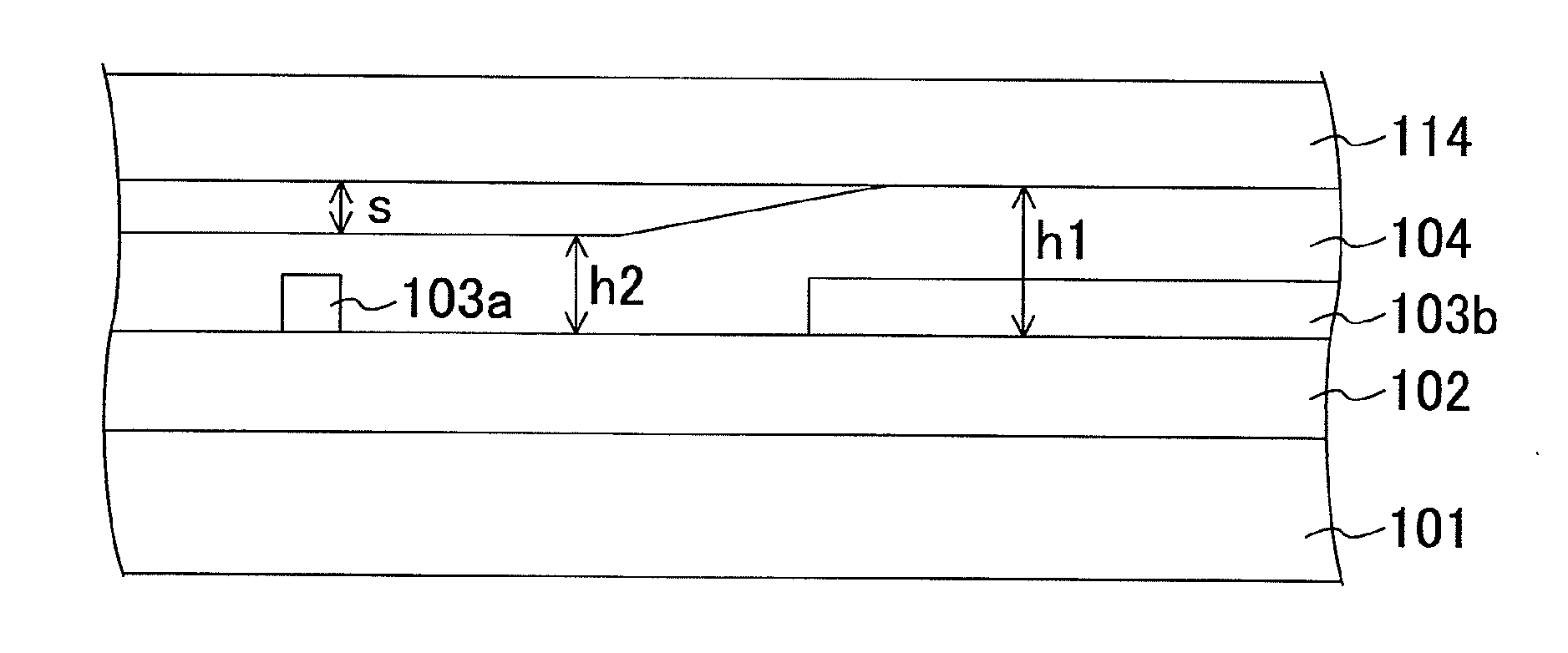
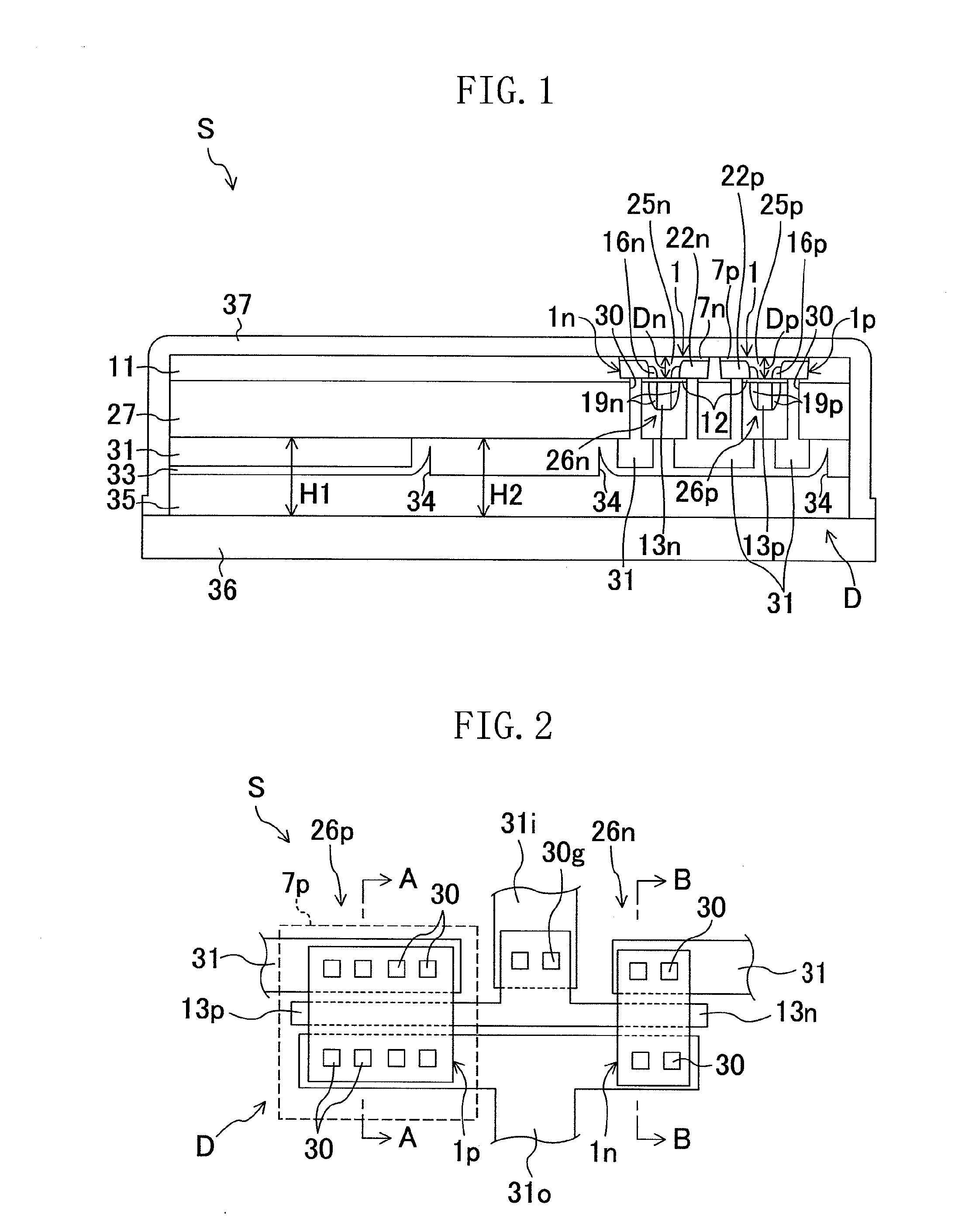
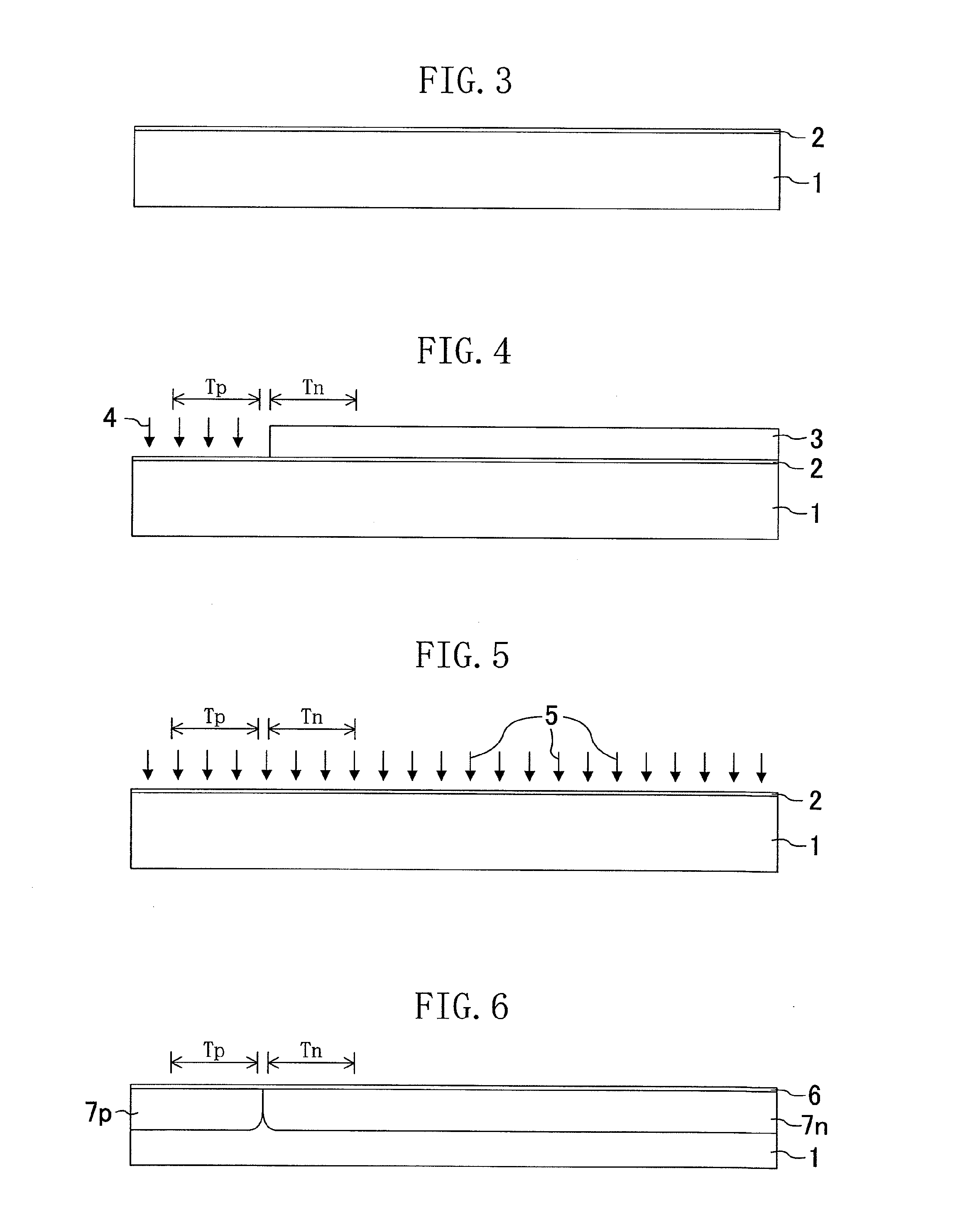
[0130]FIGS. 1 through 25 show a first embodiment of the present invention. FIG. 1 is a cross-sectional view schematically showing the structure of a main part of a semiconductor device S. FIG. 2 is a plan view schematically showing the main part of the semiconductor device S. FIGS. 3 through 25 are cross-sectional views schematically showing manufacturing steps of the semiconductor device S.
[0131]The semiconductor device S is directly formed on the glass substrate 36, which is, for example, a substrate of a display panel of an LCD device, not shown in the figure, and can be used as a driver for controlling driving of a plurality of pixels of the display panel, a power supply circuit, a memory circuit, a central processing circuit, or the like.
[0132]As shown in FIG. 1, the semiconductor device S includes a glass substrate 36, and a device portion D bonded with the glass substrate 36, and formed at a high density and with high accuracy. That is, the semiconductor device S is formed by...
second embodiment
[0201]FIGS. 26 through 29 show a second embodiment of the present invention. Note that, in the following embodiments, the same parts as those shown in FIGS. 1 through 25 are denoted by the same reference characters, and detailed description thereof will be omitted. FIGS. 26 through 29 are diagrams illustrating a device portion forming step in a manufacturing method of a semiconductor device S of the second embodiment.
[0202]In the first embodiment, the planarization assisting layer 33 is formed by entirely etching the convex portions 40 in the assisting layer forming step. However, in an assisting layer forming step of the second embodiment, the planarization assisting layer 33 is formed by partially etching the convex portions 40.
[0203]That is, in the assisting layer forming step of the second embodiment, the planarization assisting layer 33 is formed so that the height of the planarization assisting layer 33 from the surface of a first planarizing layer 27 located on the side oppos...
third embodiment
[0211]FIGS. 30 through 32 show a third embodiment of the present invention. FIGS. 30 through 32 are diagrams illustrating a device portion forming step in a manufacturing method of a semiconductor device S of the third embodiment.
[0212]In the first embodiment and the second embodiment, the device portion D, which has the surface of the second planarizing layer 35 as a bonding surface, is formed by forming the second planarizing layer 35 after the planarization assisting layer 33 is formed. However, in the third embodiment, a device portion D, which has the surface of a planarizing insulating layer 54 as a bonding surface, is formed by forming the planarizing insulating layer 54, which is an insulating layer that covers a plurality of conductive films 31.
[0213]The semiconductor device S of the present embodiment is formed by bonding the device portion D with a glass substrate 36, where the device portion D has transistors 26p, 26n formed in a substrate layer 1, a planarizing layer (c...
PUM
 Abstract
Description
Claims
Application Information
 - R&D Engineer
- R&D Manager
- IP Professional
- Industry Leading Data Capabilities
- Powerful AI technology
- Patent DNA Extraction
Browse by: Latest US Patents, China's latest patents, Technical Efficacy Thesaurus, Application Domain, Technology Topic, Popular Technical Reports.
© 2024 PatSnap. All rights reserved.Legal|Privacy policy|Modern Slavery Act Transparency Statement|Sitemap|About US| Contact US: help@patsnap.com