Flash memory device and manufacturing method of the same

a technology of flash memory and manufacturing method, which is applied in the direction of semiconductor devices, electrical equipment, basic electric elements, etc., can solve the problems of difficult removal of polysilicon covering a source region between adjacent cells, and achieve the effect of inhibiting the degradation of characteristics and minimizing the variation of cd and overlay

Inactive Publication Date: 2010-07-01
DONGBU HITEK CO LTD
View PDF1 Cites 11 Cited by
  • Summary
  • Abstract
  • Description
  • Claims
  • Application Information

AI Technical Summary

Benefits of technology

[0010]An embodiment provides a flash memory device having a self-align SONOS structure and a method for manufacturing the same, in which a self-align double spacer process is used instead of the photo and etch process to form a cell. According to embodiments, problems related to the CD and overlay variation can be minimized, thereby achieving cell uniformity while inhibiting degradation of characteristics.

Problems solved by technology

Further, referring to FIG. 1C, it can be difficult to remove polysilicon covering a source region between adjacent cells without damage when forming an active gate poly and a memory gate poly.

Method used


Image

  • Flash memory device and manufacturing method of the same
  • Flash memory device and manufacturing method of the same
  • Flash memory device and manufacturing method of the same

Examples


Embodiment Construction

[0017]Hereinafter, embodiments of a flash memory device and a method for manufacturing the same will be described with reference to accompanying drawings.

[0018]In the description of embodiments, it will be understood that when a layer (or film) is referred to as being ‘on’ another layer or substrate, it can be directly on another layer or substrate, or intervening layers may also be present. Further, it will be understood that when a layer is referred to as being ‘under’ another layer, it can be directly under another layer, or one or more intervening layers may also be present. In addition, it will also be understood that when a layer is referred to as being ‘between’ two layers, it can be the only layer between the two layers, or one or more intervening layers may also be present.

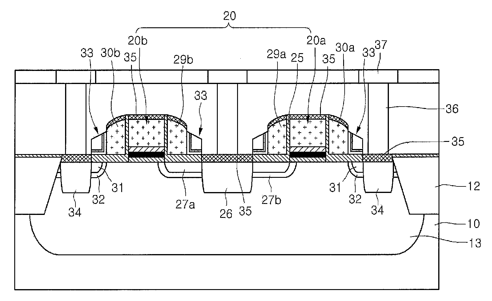
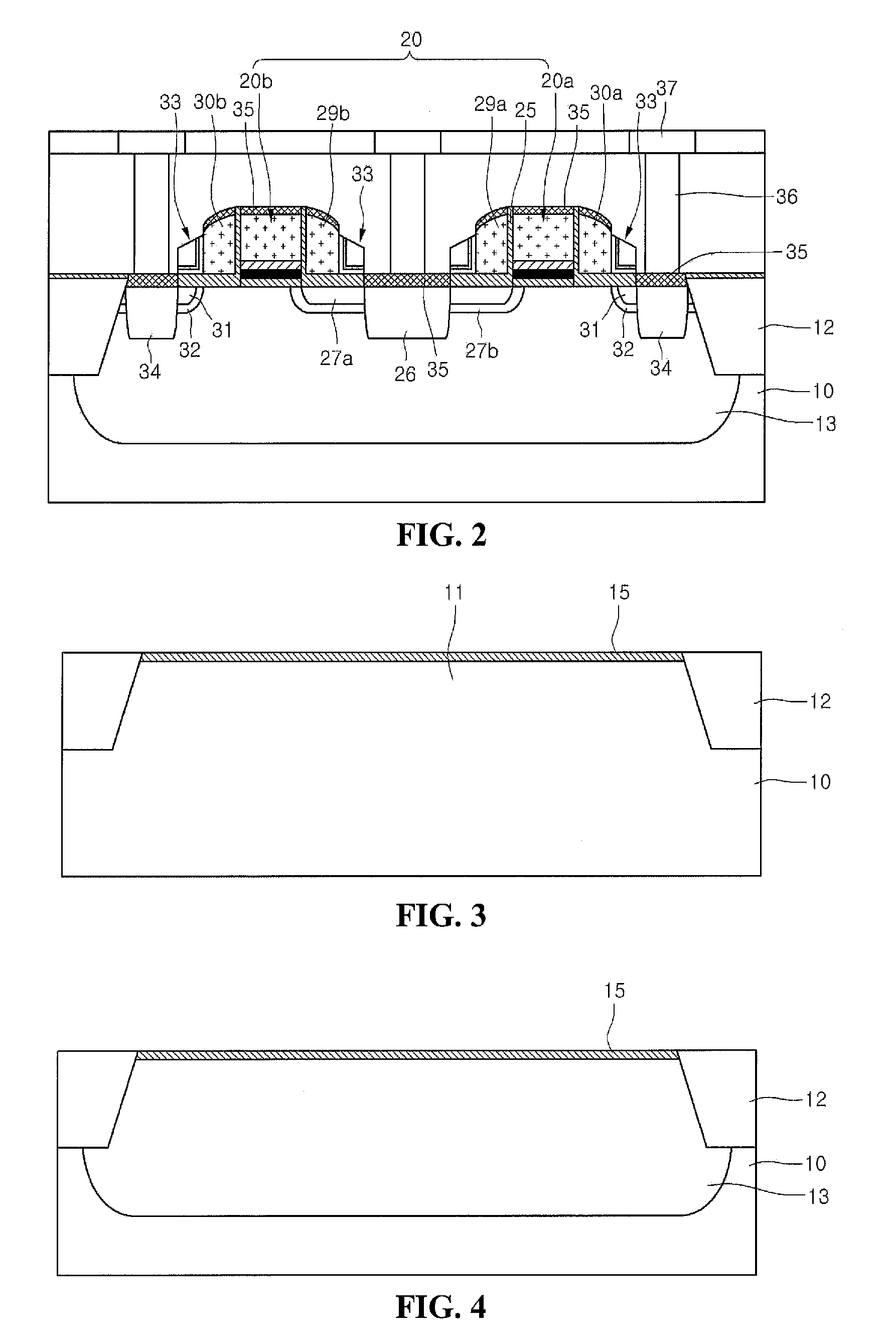
[0019]FIG. 2 is a cross-sectional view of a flash memory device according to an embodiment.

[0020]Referring to FIG. 2, flash memory device according to an embodiment includes first and second memory gates ...


PUM


Abstract

Disclosed are a flash memory device and a method for manufacturing the same. The flash memory device includes first and second memory gates on a substrate; a floating poly between the first and second memory gates; first and second select gates at respective outer sides of the first and second memory gates; an oxide layer between the first memory gate and the first select gate and between the second memory gate and the second select gate; a drain region in the substrate at outer sides of the first and second select gates; a source region in the substrate between the first and second memory gates; and a metal contact on each of the drain region and the source region.

Description

CROSS-REFERENCE TO RELATED APPLICATION[0001]This application claims the benefit under 35 U.S.C. §119 of Korean Patent Application No. 10-2008-0138887, filed Dec. 31, 2008, which is hereby incorporated by reference in its entirety.BACKGROUND[0002]A flash memory device is a nonvolatile memory device that does not lose data stored therein even if power is turned off In addition, the flash memory can record, read, and delete data at a relatively high speed.[0003]Accordingly, the flash memory device is widely used for the Bios of a personal computer (PC), a set-top box, a printer, and a network server in order to store data. Recently, the flash memory device is extensively used for digital cameras and portable phones.[0004]In such a flash memory device, a semiconductor device having a SONOS (Silicon-Oxide-Nitride-Oxide-Silicon) structure is often used.[0005]Different from a flash memory device having a floating gate including polycrystalline silicon, the SONOS memory device is a charge-t...

Claims


Application Information

Patent Timeline
Patent Type & Authority Applications(United States)
IPC IPC(8): H01L29/792H01L21/336
CPCH01L21/28273H01L21/28282H01L27/11521H01L27/11568H01L29/42328H01L29/7881H01L29/40114H01L29/40117H10B43/30H10B41/30H01L21/265H01L29/4234H01L29/792
Inventor KWON, YOUNG JUN
Owner DONGBU HITEK CO LTD
Why Eureka
Try Eureka