High-voltage metal-oxide-semiconductor device

a high-voltage metal-oxidesemiconductor and device technology, applied in the direction of semiconductor devices, basic electric elements, electrical equipment, etc., can solve the problem that the above-described high-voltage nmos device b>101/b> cannot be operated, and achieve the effect of improving the structure of the hvmos devi

Inactive Publication Date: 2010-07-01
MEDIATEK INC
View PDF9 Cites 14 Cited by
  • Summary
  • Abstract
  • Description
  • Claims
  • Application Information

AI Technical Summary

Benefits of technology

[0008]It is one objective of this invention to provide an improved HVMOS device structure that is COMS compatible and is operable when the drain terminal is negatively biased.
[0009]It is another objective of this invention to provide an improved HVMOS device structure with improved time dependent dielectric breakdown (TDDB) characteristic and reduced hot carrier injection (HCI) effect.

Problems solved by technology

However, the above-described high-voltage NMOS device 101 cannot be operated when the drain is negatively biased because the junction between the DNW 110 and the P type substrate 100 will be turned on and thus causes leakage.

Method used


Image

  • High-voltage metal-oxide-semiconductor device
  • High-voltage metal-oxide-semiconductor device
  • High-voltage metal-oxide-semiconductor device

Examples


Embodiment Construction

[0021]The present invention has been particularly shown and described with respect to certain embodiments and specific features thereof. The embodiments set forth hereinbelow are to be taken as illustrative rather than limiting. It should be readily apparent to those of ordinary skill in the art that various changes and modifications in form and detail may be made without departing from the spirit and scope of the invention.

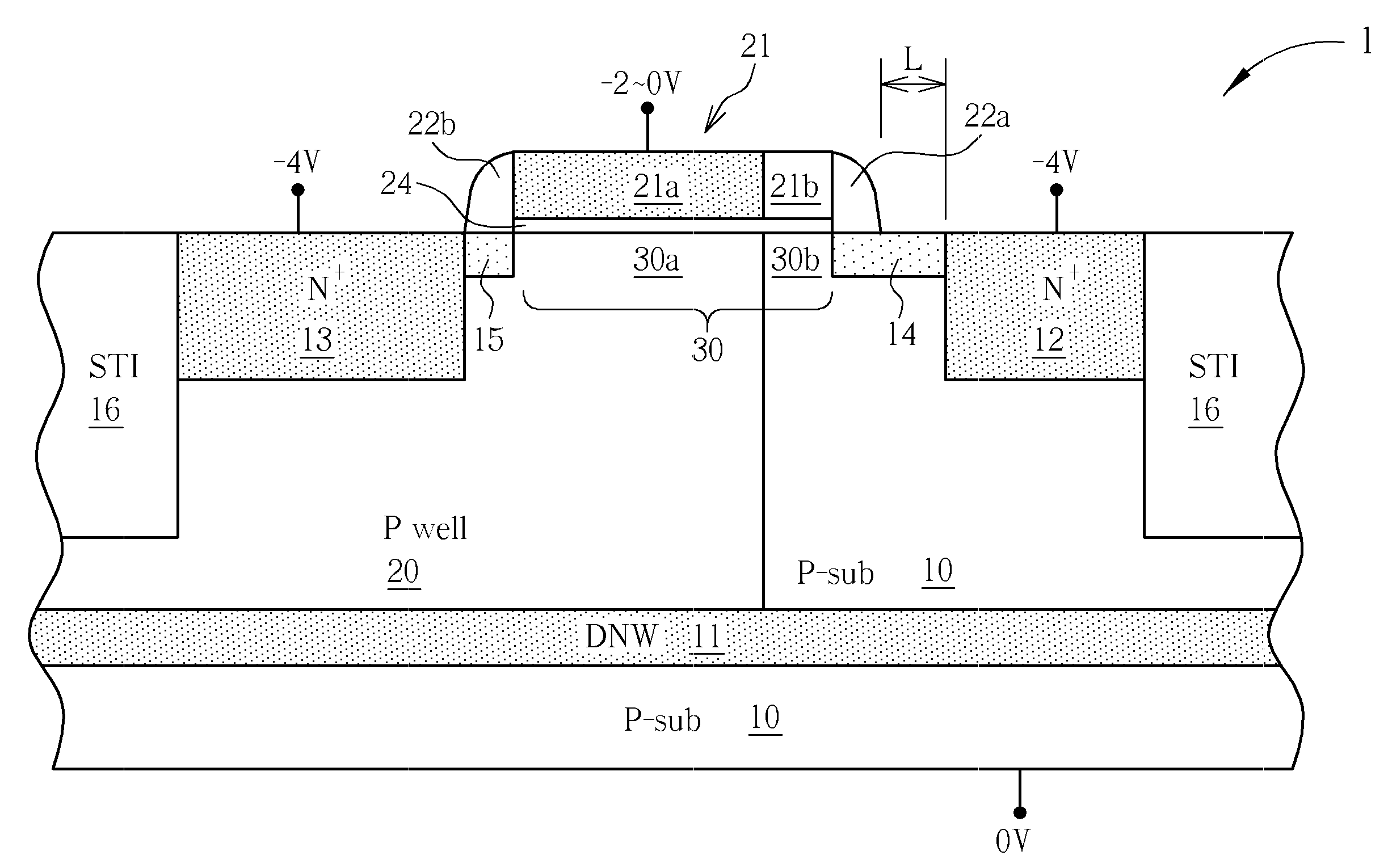
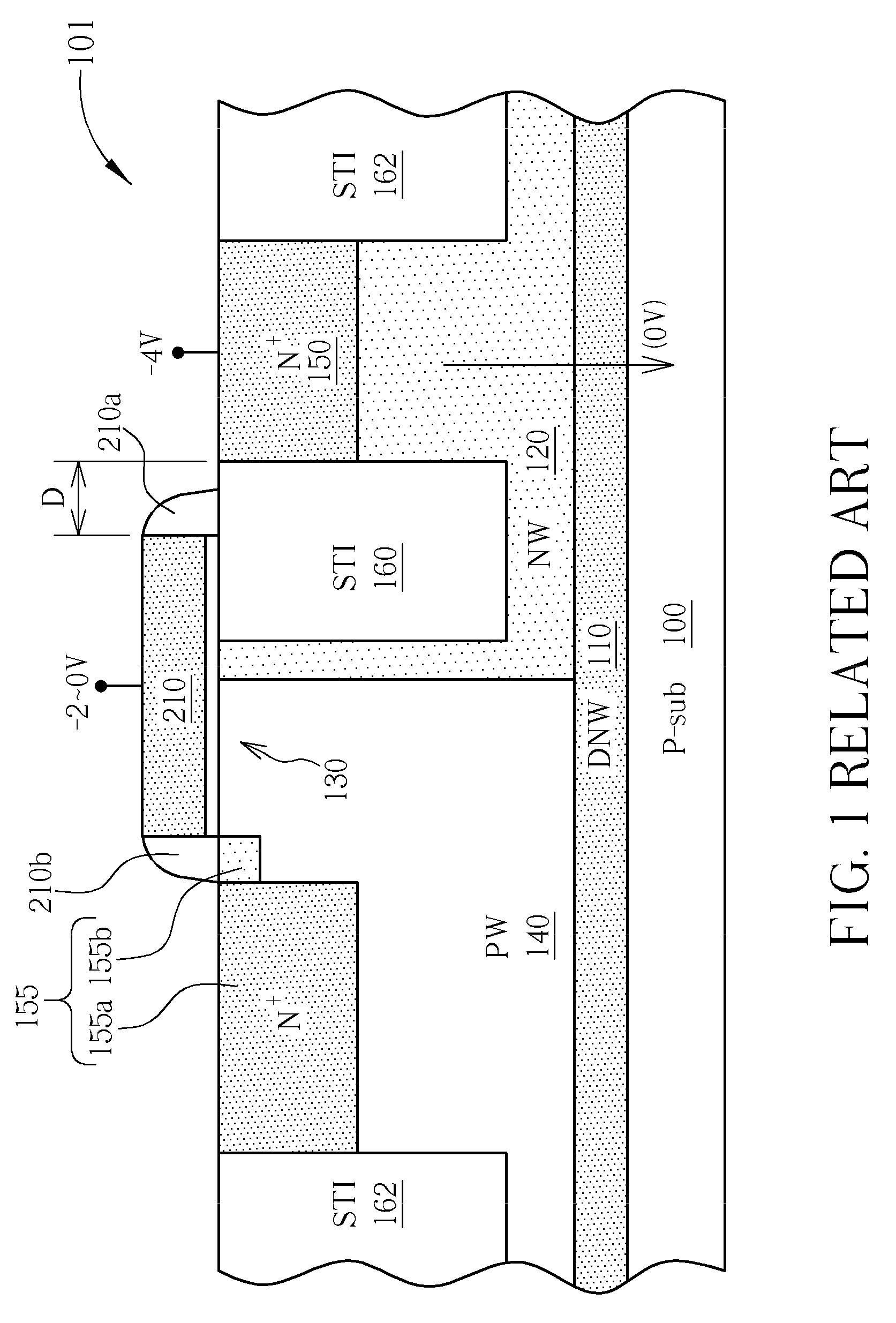
[0022]The exemplary structures of HVMOS transistor according to the present invention are described in detail. The improved HVMOS transistor structure is described for a high-voltage NMOS transistor, but it should be understood by those skilled in the art that by reversing the polarity of the conductive dopants high-voltage PMOS transistors can be made.

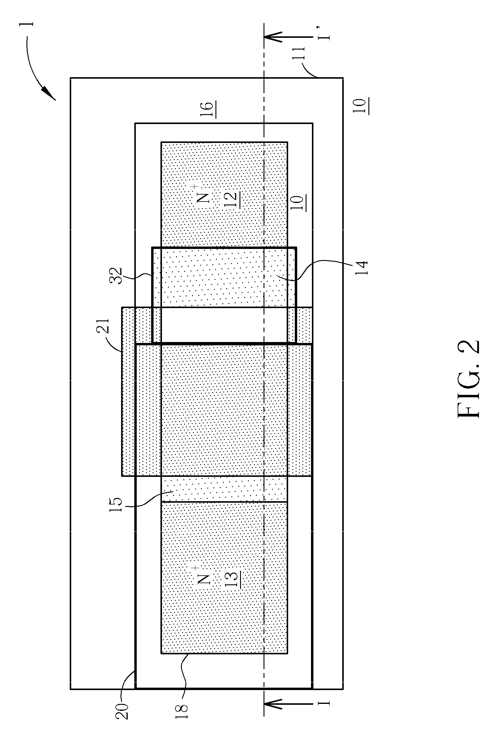
[0023]FIG. 2 is an exemplary layout of the improved high-voltage NMOS transistor structure in accordance with one embodiment of this invention. FIG. 3 is a schematic, cross-sectional view taken alone line I-I′ of F...


PUM


Abstract

A high-voltage MOS transistor includes a gate overlying an active area of a semiconductor substrate; a drain doping region pulled back away from an edge of the gate by a distance L; a first lightly doped region between the gate and the drain doping region; a source doping region in a first ion well; and a second lightly doped region between the gate and the source doping region.

Description

BACKGROUND OF THE INVENTION[0001]1. Field of the Invention[0002]The present invention relates to a high-voltage device structure. More particularly, the present invention relates to a high-voltage metal-oxide-semiconductor (HVMOS) device structure.[0003]2. Description of the Prior Art[0004]High-voltage metal-oxide-semiconductors are MOS devices for use under high voltages, which may be, but not limited to, voltages higher than the voltage supplied to the I / O circuit. HVMOS devices may function as switches and are broadly utilized in audio output drivers, CPU power supplies, power management systems, AC / DC converters, LCD or plasma television drivers, automobile electronic components, PC peripheral devices, small DC motor controllers, and other consumer electronic devices.[0005]FIG. 1 is a schematic, cross-sectional view of a conventional high-voltage NMOS device. As shown in FIG. 1, the high-voltage NMOS device 101 includes a gate 210 overlying an area of a P type substrate 100, a d...

Claims


Application Information

Patent Timeline
Patent Type & Authority Applications(United States)
IPC IPC(8): H01L29/78
CPCH01L29/0692H01L29/0847H01L29/1045H01L29/7835H01L29/4983H01L29/7833H01L29/1083
Inventor LEE, MING-CHENGCHENG, TAOYANG, MING-TZONG
Owner MEDIATEK INC
Why Eureka
Try Eureka