

Semiconductor device and power converter using the same
a technology of semiconductor devices and power converters, applied in power conversion systems, pulse techniques, electronic switching, etc., can solve the problems of increasing the area increasing the number of parts, and reducing the integration difficulty of the driving circuit, so as to increase the current driving capacity of the device, increase the current driving capacity, and reduce the size of the device
- Summary
- Abstract
- Description
- Claims
- Application Information
AI Technical Summary
Benefits of technology
Problems solved by technology
Method used
Image

Examples
second embodiment
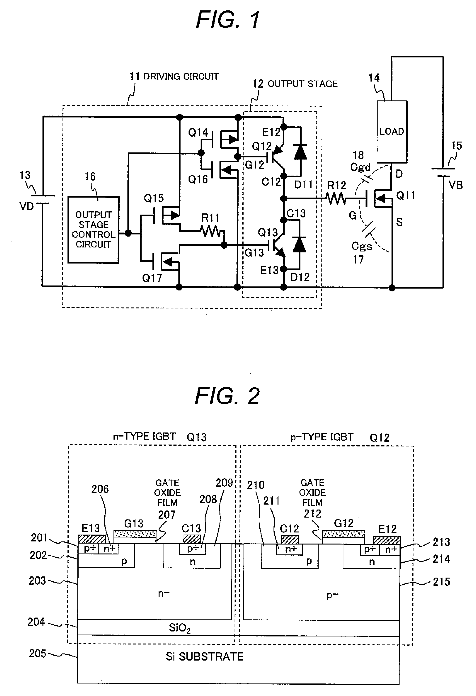
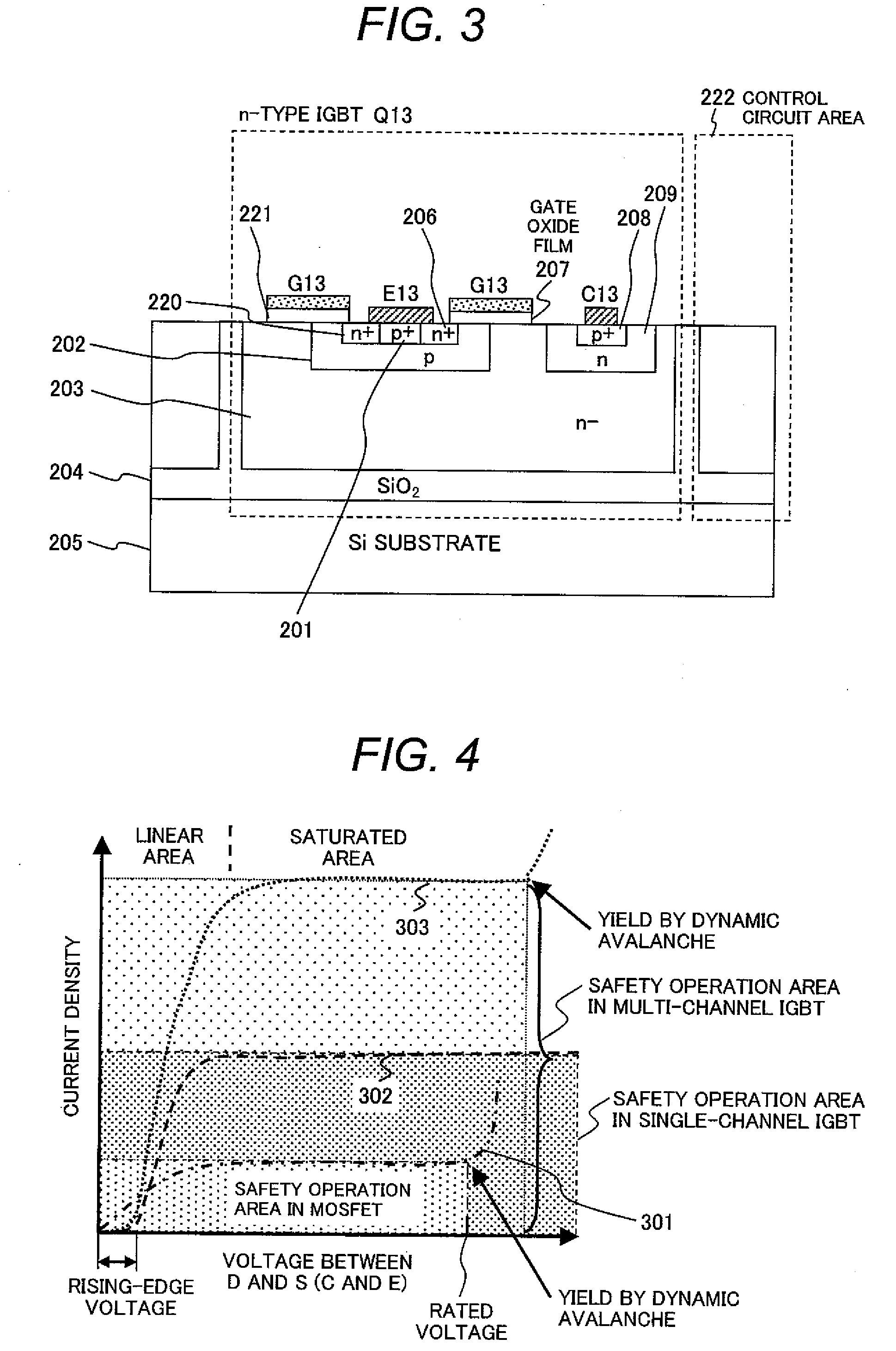
[0035]The second embodiment shown in FIG. 3 is a multi-channel IGBT in which the gate G13 of the IGBT is provided at both sides of the emitter E13 so that two channels are formed for a single collector C13 to increase the gate capacity. With the IGBT of this type, a saturated current two times higher than the characteristic curve 302 of the single-channel IGBT is obtained, as indicated by the characteristic curve 303 in FIG. 4. As the number of channels is increased, the driving capacity can be further optimized.
[0036]Even if an insulated gate thyristor, which is another insulated gate bipolar device, is used as the device at the output stage, the same effect as when the IGBT is used at the output stage can be obtained.
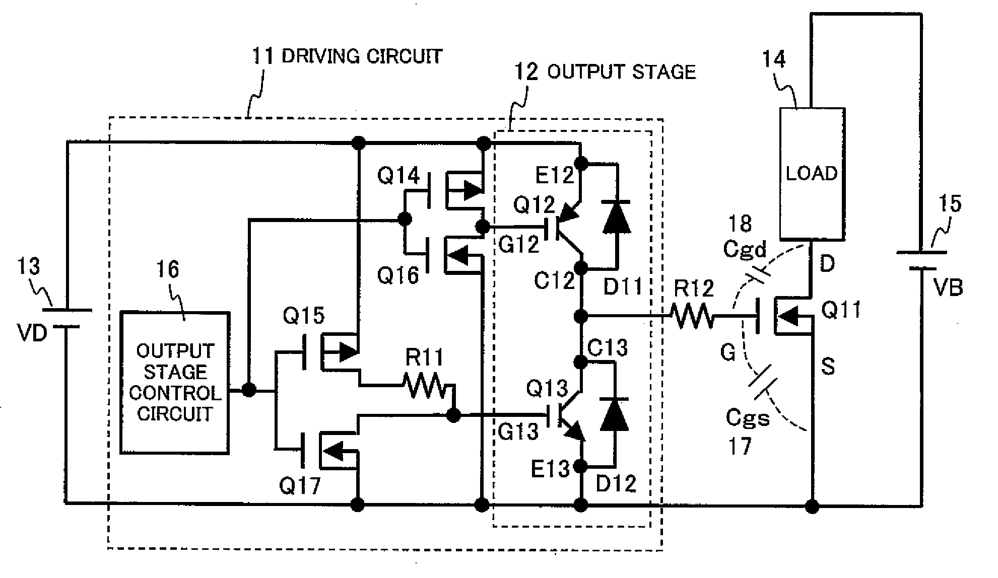
[0037]As described above, the present invention can improve the current driving capacity of the device at the output stage and can easily integrate the circuit at the output stage, in which individual devices have needed to be used.
[0038]When the current driving capac...
third embodiment
[0039]FIG. 5 is a cross sectional view showing the structure of a semiconductor in a semiconductor device in the present invention. In this embodiment, only the structure of an n-type IGBT corresponding to the n-type IGBT in FIG. 2 is shown; a p-type IGBT corresponding to Q12 is omitted. In the drawing, reference numeral 401 indicates a back gate power supply p+ layer, 402 indicates a p-type channel layer, 403 indicates an n-type active Si layer, 404 indicates a buried oxide film for device isolation, and 405 indicates a Si support substrate, which is a dielectric isolation substrate. Reference numeral 406 indicates an emitter n+ layer, 407 indicates a gate oxide film, 408 indicates a collector p+ layer, 409 indicates an n-type buffer layer, 410 indicates an n+ layer for buffer layer power supply, 411 indicates an emitter electrode, 413 indicates a collector electrode, and 414 indicates a gate electrode.
[0040]In this embodiment, the n+ layer 410 formed in the n-type buffer 409 of th...
fourth embodiment
[0042]FIG. 6 shows the circuit in a semiconductor device in the present invention. This embodiment is achieved by replacing the p-type IGBT Q12 at the output stage in the embodiment in FIG. 1 with an n-type IGBT Q52. The gate withstand voltages of IGBTs Q52 and Q53 are lower than the voltage of the gate power supply VD. In this embodiment, the voltage of a gate power supply VC 57 of IGBT Q53 at the output stage is lower than the voltage of the gate power supply VD of the main switching device. Specifically, the voltage of the gate power supply VC is assumed to be about 5V; by comparison, the voltage of the gate power supply VD is about 15V. The degree of majority carrier movement in the n-type IGBT is higher than in the p-type IGBT, enabling the current driving capacity to be approximately doubled. To drive an n-type IGBT, a power supply generating a voltage higher than the voltage of the gate power supply VD is generally required to drive the gate. In this embodiment, however, an o...
PUM
 Abstract
Description
Claims
Application Information