Semiconductor memory device having auto-precharge function

a memory device and memory technology, applied in the field of memory devices of semiconductors, can solve the problems of large power consumption of drams and conventional synchronous drams, and achieve the effect of preventing unnecessary power consumption

Active Publication Date: 2010-07-01
LONGITUDE LICENSING LTD
View PDF3 Cites 41 Cited by
  • Summary
  • Abstract
  • Description
  • Claims
  • Application Information

AI Technical Summary

Benefits of technology

[0013]According to the present invention, the second internal clock used for counting a write recovery period is generated separately from the first internal clock used for counting latency. When auto-precharge is not designated, the second internal clock is deactivated (stopped). Accordingly, when the auto-precharge function is not used, the second counter does not perform any counting operation. Therefore, it is possible to prevent unnecessary power consumption.

Problems solved by technology

However, conventional synchronous DRAMs have the following problems.
As a result, the DRAM consumes large power when the auto-precharge function is not operated.

Method used


Image

  • Semiconductor memory device having auto-precharge function
  • Semiconductor memory device having auto-precharge function
  • Semiconductor memory device having auto-precharge function

Examples


first embodiment

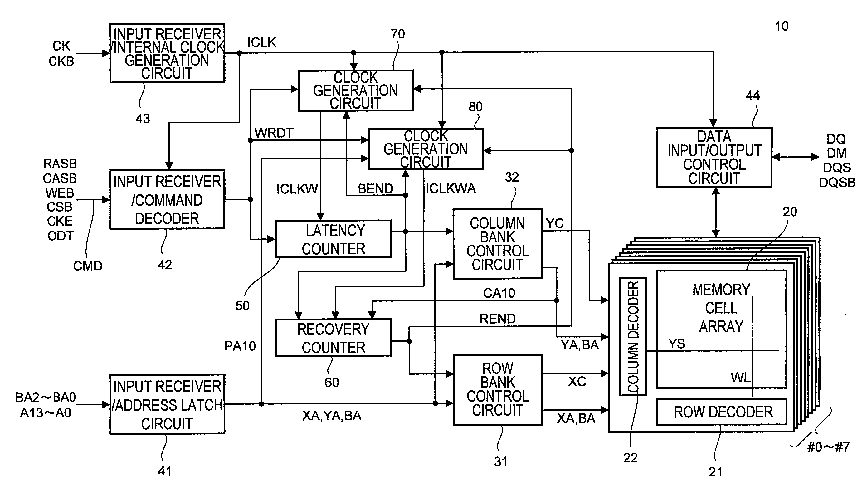
[0025]FIG. 1 is a block diagram showing a configuration of a semiconductor memory device 10 according to the present invention.

[0026]As shown in FIG. 1, the semiconductor memory device 10 according to the first embodiment includes a memory cell array 20 that includes banks #0 to #7, a row decoder 21 that selects a row of the memory cell array 20, and a column decoder 22 that selects a column of the memory cell array 20.

[0027]A row address XA, a bank address BA, and a row control signal XC are supplied to the row decoder 21 from a row bank control circuit 31. Based on the addresses and signal, the row decoder 21 selects a word line WL included in the memory cell array 20. A column address YA, a bank address BA, and a column control signal YC are supplied to the column decoder from a column bank control circuit 32. Based on the addresses and signal, the column decoder 22 selects a column selection line YS. The column selection line YS is a signal for selecting a bit line BL included i...

second embodiment

[0062]the present invention is explained next.

[0063]FIG. 7 is a block diagram showing a semiconductor memory device 100 according to the second embodiment.

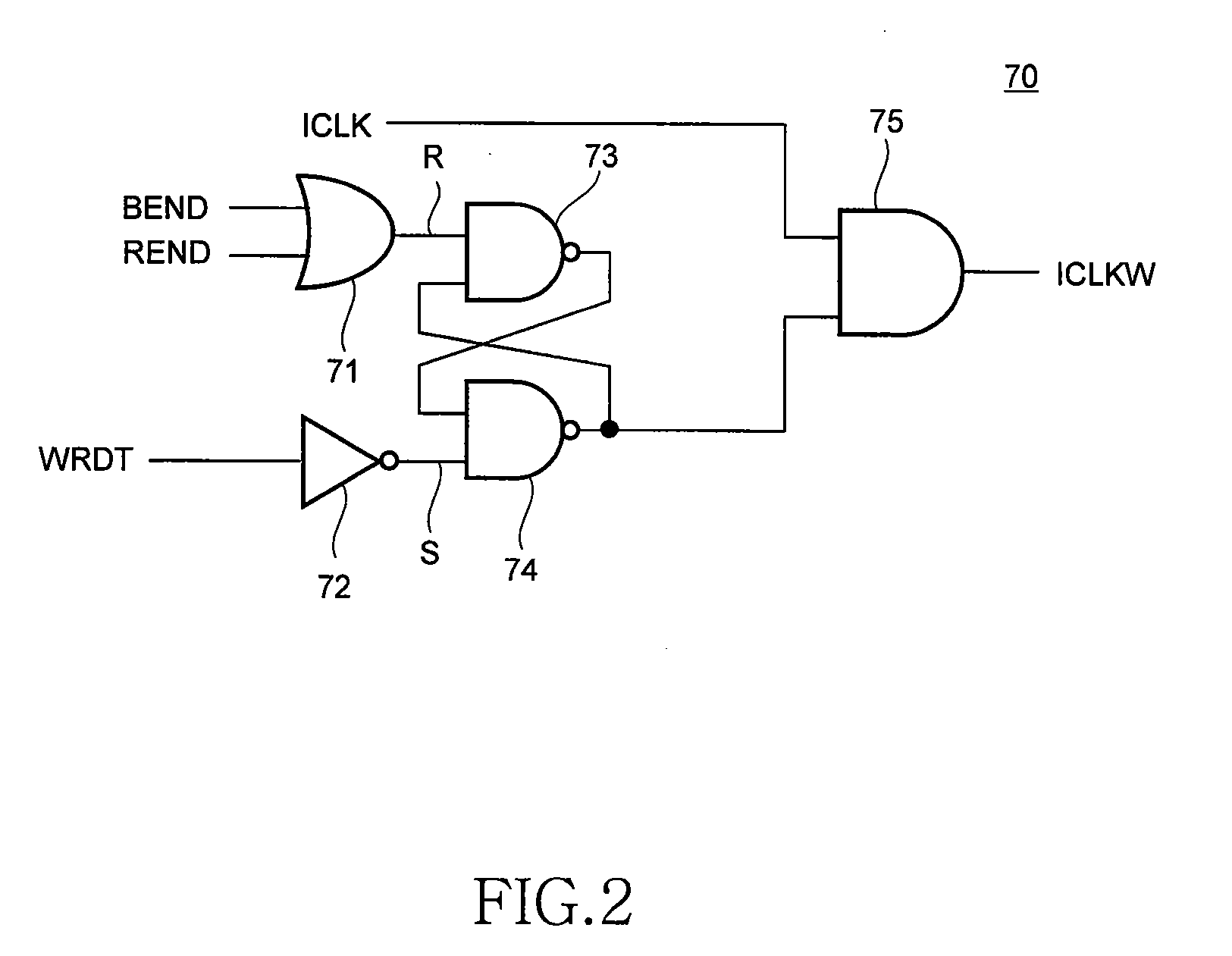
[0064]The semiconductor memory device 100 according to the second embodiment differs from the semiconductor memory device 10 shown in FIG. 1 in that the clock generation circuit 80 that generates the internal clock ICLKWA is replaced by a clock generation circuit 90. An internal clock ICLK, a recovery end signal REND, an auto-precharge designation signal CA10, and an internal write command WRCT are supplied to the clock generation circuit 90. Differently from the clock generation circuit 80 according to the first embodiment, the burst end signal BEND, an auto-precharge designation signal PA10, and the internal write command WRDT are not input to the clock generation circuit 90.

[0065]FIG. 8 is a circuit diagram of the clock generation circuit 90.

[0066]As shown in FIG. 8, the clock generation circuit 90 is configured to include NAND...


PUM


Abstract

To provide a semiconductor memory device including: a first clock generation circuit and a second clock generation circuit that generate a first internal clock and a second internal clock, respectively; a latency counter that counts latency synchronously with the first internal clock; and a recovery counter that counts a write recovery period synchronously with the second internal clock. The second clock generation circuit activates the second internal clock when auto-precharge is designated, and deactivates the second internal clock when the auto-precharge is not designated. With this configuration, the recovery counter does not perform any counting operation when an auto-precharge function is not operated, and thus unnecessary power consumption can be prevented.

Description

BACKGROUND OF THE INVENTION[0001]1. Field of the Invention[0002]The present invention relates to a semiconductor memory device, and more particularly relates to a semiconductor memory device including an auto-precharge function for automatically resetting a word line and of precharging a bit line after ending a read operation or a write operation.[0003]2. Description of Related Art[0004]An operation performed by a synchronous DRAM (Dynamic Random Access Memory), which is a representative semiconductor memory device, is controlled based on a command and an address issued synchronously with an external clock signal. Specifically, when a row address is supplied to a synchronous DRAM synchronously with an active command and then a column address is supplied thereto synchronously with a read command, read data is output from the DRAM after passage of CAS latency since an input of the read command. Furthermore, when a row address is supplied to the DRAM synchronously with an active comman...

Claims


Application Information

Patent Timeline
Patent Type & Authority Applications(United States)
IPC IPC(8): G11C7/00G11C8/18G11C8/00
CPCG11C11/4076G11C11/4094
Inventor KUROKI, KOJI
Owner LONGITUDE LICENSING LTD
Why Eureka
Try Eureka