Semiconductor device and method of making the same
a technology of semiconductor devices and semiconductors, applied in the direction of semiconductor/solid-state device details, radiation control devices, instruments, etc., can solve the problem of complicated wire layout, and achieve the effect of simplifying the wire layou
- Summary
- Abstract
- Description
- Claims
- Application Information
AI Technical Summary
Benefits of technology
Problems solved by technology
Method used
Image

Examples
first embodiment
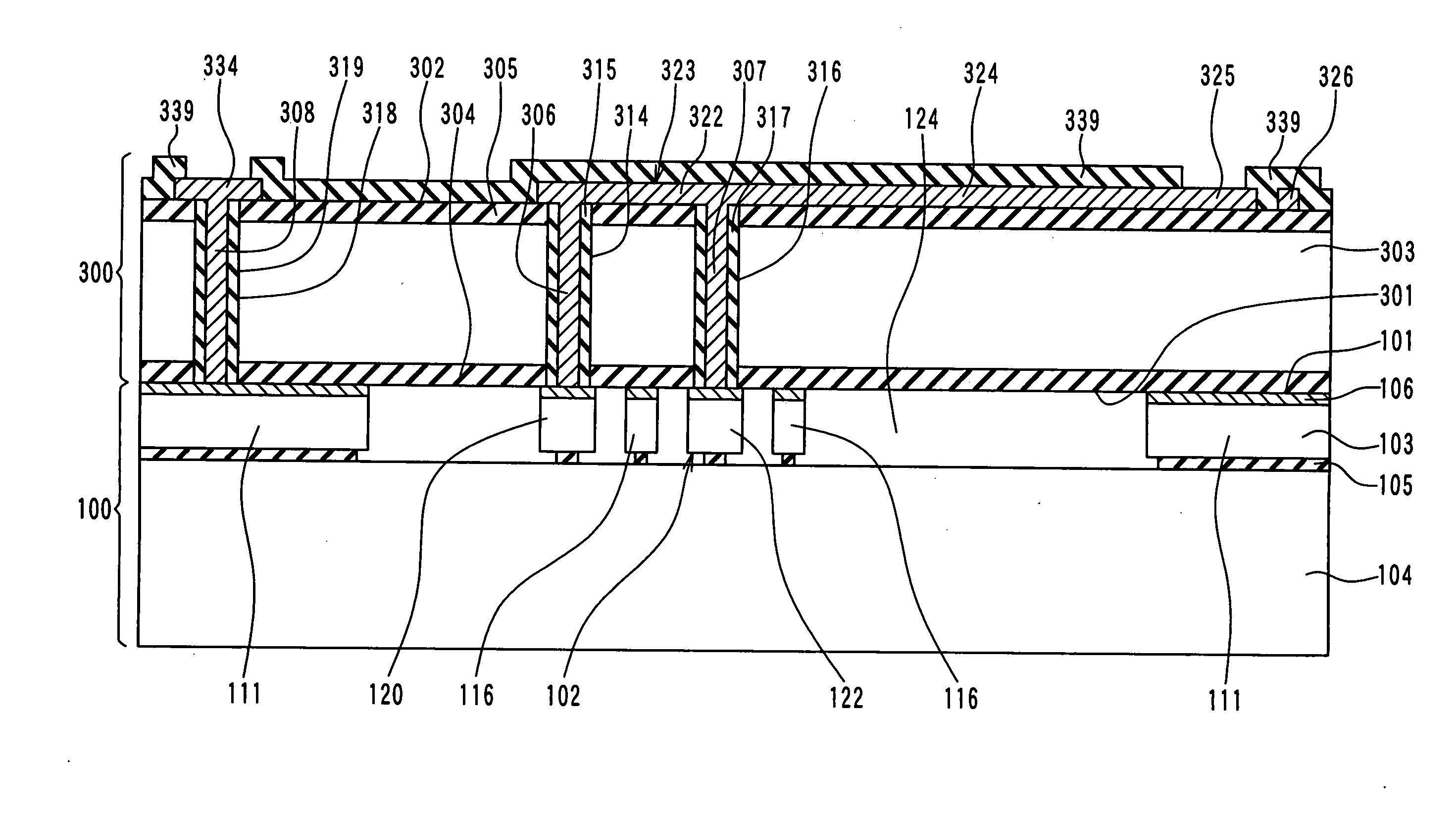
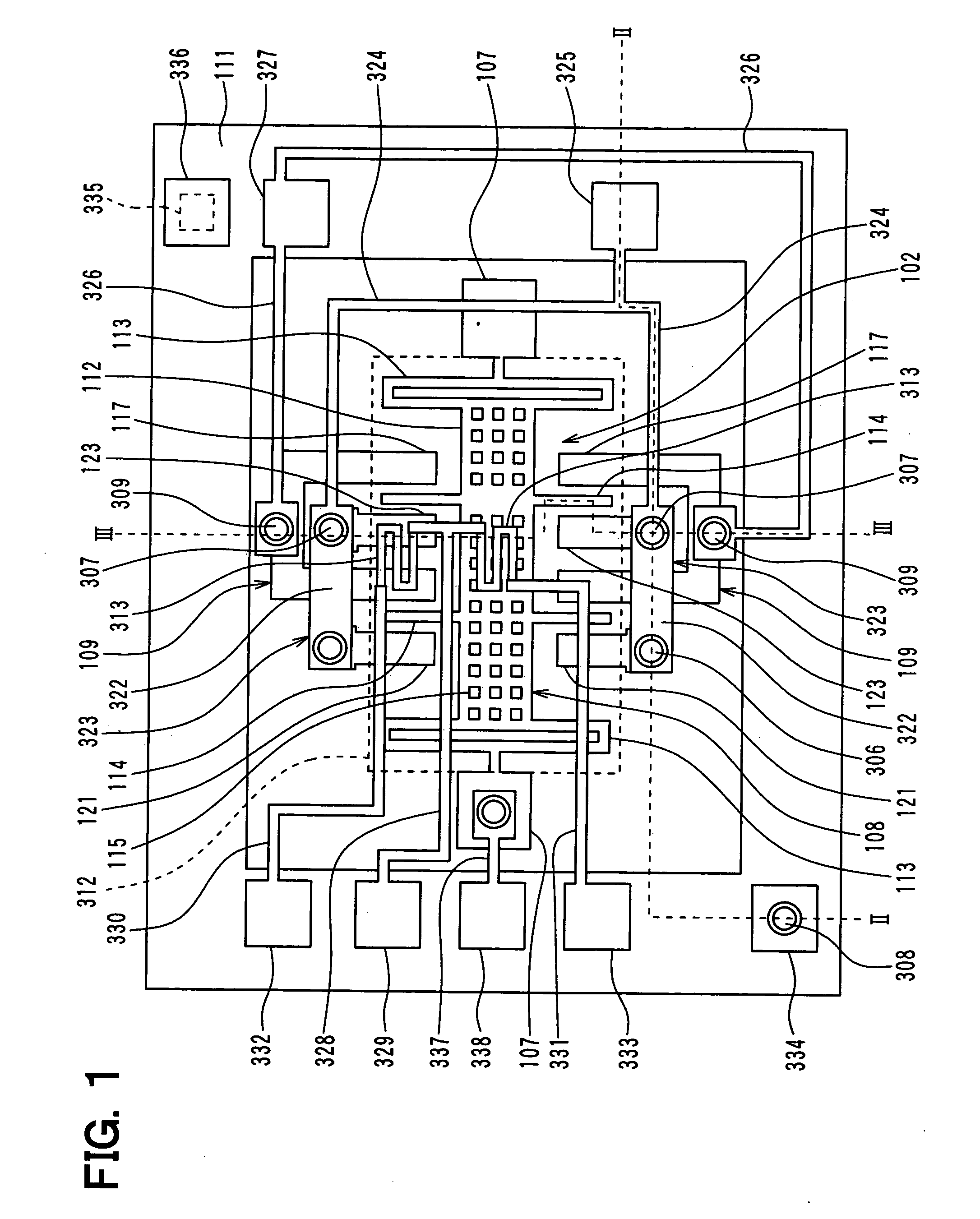
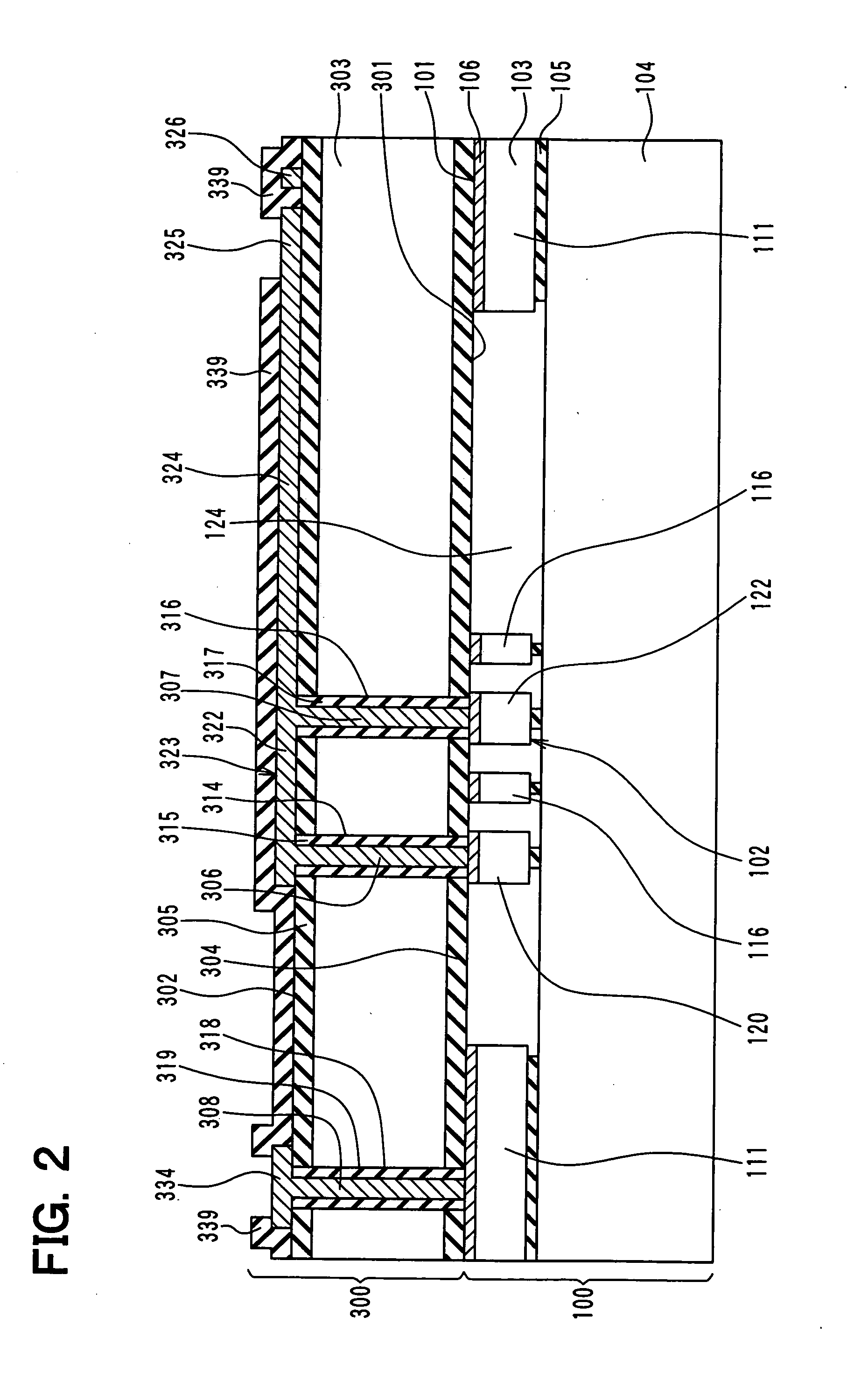
[0056]A semiconductor device according to a first embodiment of the present invention is described below with reference to FIGS. 1-3. FIG. 1 is a plan view of the semiconductor device. FIG. 2 is a cross-sectional view taken along, the line II-II in FIG. 1. FIG. 3 is a cross-sectional view taken along the line in FIG. 1.
[0057]As shown in FIGS. 2 and 3, the semiconductor device includes a sensor member 100 and a cap member 300 stacked on the sensor member 100. The sensor member 100 is shaped like a plate and has a surface 101. The cap member 300 is shaped like a plate and has first and second surfaces 301, 302 opposite to each other. The sensor member 100 and the cap member 300 are joined together to form the semiconductor device.
[0058]The sensor member 100 has a first sensing section 102 on the surface 101 side. The first sensing section 102 is configured to detect a physical quantity such as an acceleration or an angular velocity. The sensor member 100 is formed with a silicon-on-in...
second embodiment
[0125]A semiconductor device according to a second embodiment of the present invention is discussed below with reference to FIGS. 9-11. FIG. 9 is a plan view of the semiconductor device, FIG. 10 is a cross-sectional view taken along the line. X-X in FIG. 9, and FIG. 11 is a cross-sectional view taken along the line XI-XI in FIG. 9. A difference of the second embodiment with respect to the first embodiment is summarized as follows. According to the first embodiment, the cross wire 322 is formed on the insulation layer 305. In contrast, according to the second embodiment, the cross wire 322 is formed on the insulation layer 304.
[0126]The sensor member 100 of the second embodiment has the same structure as the sensor member 100 of the first embodiment. Therefore, a planar layout of the sensor member 100 shown in FIG. 9 is the same as a planar layout of the sensor member 100 shown in FIG. 4. However, unlike the first embodiment, the ion-implanted layer 106 is not formed in the surface p...
third embodiment
[0156]A semiconductor device according to a third embodiment of the present invention is discussed below with reference to FIG. 15. A difference of the third embodiment with respect to the preceding embodiments is summarized as follows. According to the third embodiment, the cross wiring portion 323 is located on the first surface 301 side of the cap member 300, and an integrated circuit portion instead of the second sensing section 310 is formed in the cap member 300.
[0157]FIG. 15 is a cross-sectional view of the semiconductor device taken along the line XI-XI in FIG. 9. As shown in FIG. 15, an integrated circuit portion 360 is formed in the silicon substrate 303 of the cap member 300. The IC portion 360 performs signal processing on a detection signal of the first sensing section 102.
[0158]The IC portion 360 is formed in a surface portion of the silicon substrate 303 on the second surface side. The IC portion 360 is formed in the silicon substrate 303 by a typical semiconductor ma...
PUM
 Abstract
Description
Claims
Application Information
 - Generate Ideas
- Intellectual Property
- Life Sciences
- Materials
- Tech Scout
- Unparalleled Data Quality
- Higher Quality Content
- 60% Fewer Hallucinations
Browse by: Latest US Patents, China's latest patents, Technical Efficacy Thesaurus, Application Domain, Technology Topic, Popular Technical Reports.
© 2025 PatSnap. All rights reserved.Legal|Privacy policy|Modern Slavery Act Transparency Statement|Sitemap|About US| Contact US: help@patsnap.com