Semiconductor device and method of fabricating the same

a technology of semiconductor devices and semiconductor resins, applied in semiconductor devices, semiconductor/solid-state device details, electrical apparatus, etc., can solve problems such as increasing the size of circuit boards, and achieve the effect of reducing the stress originating from the thermal contraction of filling resins

Active Publication Date: 2010-07-15
SONY CORP
View PDF1 Cites 6 Cited by
  • Summary
  • Abstract
  • Description
  • Claims
  • Application Information

AI Technical Summary

Benefits of technology

[0013]In the method of fabricating a semiconductor device according to this embodiment of the invention, when the filling resin is filled between the mount body and the semiconductor chip, the area which becomes wetted by the filling resin is restricted by the resin stop portion. Accordingly, the filling resin is stopped by the resin stop portion to stay inside the chip mount area. Therefore, the contact area between the mount body and the filling resin becomes narrower as compared with a case where a resin fillet is formed all aro

Problems solved by technology

This inevitably increases th

Method used


Image

  • Semiconductor device and method of fabricating the same
  • Semiconductor device and method of fabricating the same
  • Semiconductor device and method of fabricating the same

Examples


first embodiment

1. First Embodiment

Fabrication Method for Semiconductor Device

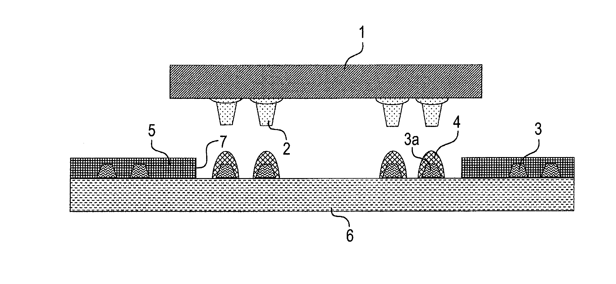
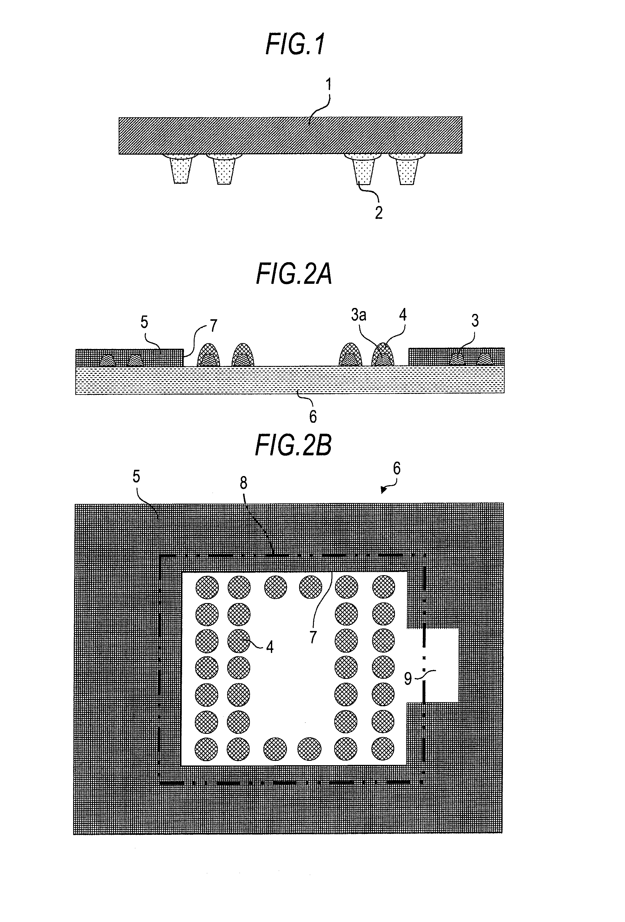
[0044]A fabrication method for a semiconductor device according to the first embodiment of the invention will be described. The fabrication method for a semiconductor device mainly includes a chip fabrication step, a board fabrication step, a chip mounting step, and a sealing step. Either one of the chip fabrication step and the board fabrication step may be executed earlier, or both steps may be executed in parallel.

(Chip Fabrication Step)

[0045]In the chip fabrication step, as shown in FIG. 1, a semiconductor chip 1 having projecting (convex) connecting terminals 2 is fabricated. The semiconductor chip 1 is formed of, for example, silicon as a main material, and each chip is diced from a semiconductor wafer whose back side is polished to have a predetermined thickness. The semiconductor chip 1 is formed into a quadrangle (square or rectangle) as viewed planarly. Unillustrated devices, wirings, etc. are formed in the majo...

second embodiment

2. Second Embodiment

Fabrication Method for Semiconductor Device

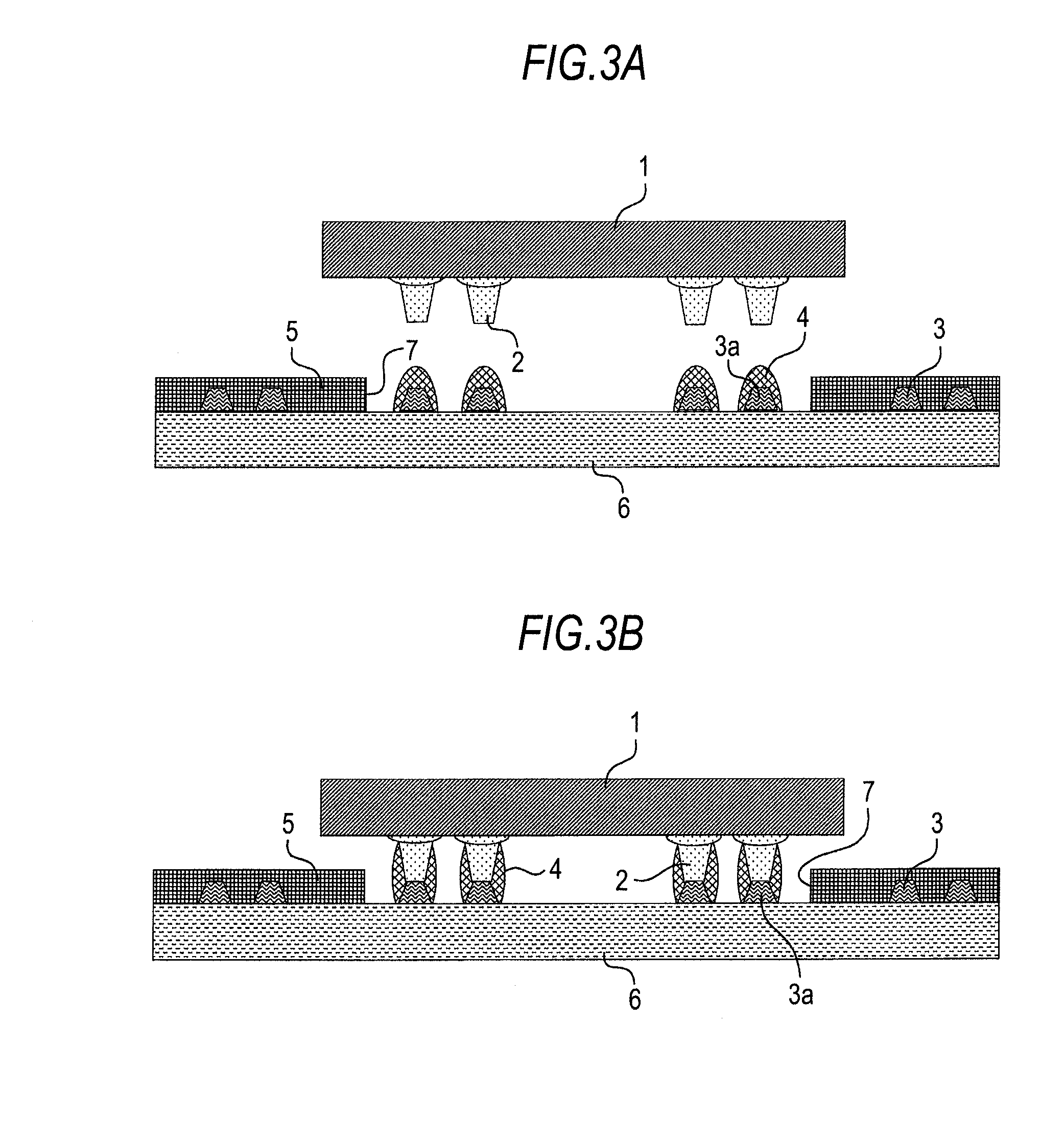
[0057]A fabrication method for a semiconductor device according to the second embodiment of the invention will be described. The fabrication method for a semiconductor device mainly includes a chip fabrication step, a board fabrication step, a chip mounting step, and a sealing step. Either one of the chip fabrication step and the board fabrication step may be executed earlier, or both steps may be executed in parallel. The second embodiment of the invention will be described with same reference numerals given to those portions which are the same as the corresponding portions of the first embodiment.

(Chip Fabrication Step)

[0058]In the chip fabrication step, as shown in FIG. 6, a semiconductor chip 1 having projecting (convex) connecting terminals 2 is fabricated. The semiconductor chip 1 is formed of, for example, silicon as a main material, and each chip is diced from a semiconductor wafer whose back side is polished to ...

third embodiment

3. Third Embodiment

[0068]FIGS. 11A and 11B are diagrams showing the configuration of a semiconductor device according to the third embodiment of the invention; FIG. 11A is a cross-sectional view, and FIG. 11B is a plan view. The third embodiment of the invention differs from the above-described second embodiment in that the annular resin stop portion 7 is provided in double on the major surface of the circuit board 6. The resin stop portion 7 is provided in double inward of the chip mount area 8 on the circuit board 6 where the semiconductor chip 1 is to be mounted. The double resin stop portions 7 are arranged concentrically to surround the area where the plurality of connecting terminals 2 are arranged. The resin stop portion 7 is formed in double by patterning the protection layer 5 in the board fabrication step.

[0069]According to the third embodiment of the invention, the resin stop portion 7 is formed in double on the major surface of the circuit board 6 at the inner and outer ...


PUM


Abstract

A semiconductor device includes: a mount body; a semiconductor chip mounted on the mount body via projecting connecting terminals; and a filling resin filled between the mount body and the semiconductor chip to seal the connecting terminals, the filling resin being retained inside the semiconductor chip in such a way as not to run out of at least one side portion in four side portions defining an outer peripheral portion of the semiconductor chip.

Description

[0001]The present application contains subject matter related to that disclosed in Japanese Priority Patent Application JP 2009-006282 filed in the Japan Patent Office on Jan. 15, 2009, the entire contents of which is hereby incorporated by reference.BACKGROUND OF THE INVENTION[0002]1. Field of the Invention[0003]The present invention relates to a semiconductor device and a method of fabricating the same. Particularly, the invention relates to a semiconductor device having a semiconductor chip mounted on a mount body, and a method of fabricating the same.[0004]2. Description of the Related Art[0005]One of semiconductor devices known has a semiconductor chip mounted on a circuit board in a flip chip form. In this type of semiconductor device, the circuit board and the semiconductor chip are connected together electrically and mechanical via connecting terminals called bumps. To protect the connecting terminals, a filling resin called “underfill material” is filled between (in a cavit...

Claims


Application Information

Patent Timeline
IPC IPC(8): H01L23/48H01L21/50
CPCH01L21/563H01L21/565H01L23/3128H01L23/49811H01L23/49838H01L24/12H01L24/16H01L24/17H01L24/28H01L24/32H01L24/81H01L24/83H01L25/03H01L25/0657H01L2224/1132H01L2224/1134H01L2224/1308H01L2224/13082H01L2224/13083H01L2224/13111H01L2224/13144H01L2224/13147H01L2224/13155H01L2224/13166H01L2224/16145H01L2224/16225H01L2224/27013H01L2224/48091H01L2224/48227H01L2224/73203H01L2224/81121H01L2224/81193H01L2224/81801H01L2224/83051H01L2224/83101H01L2224/838H01L2225/0651H01L2225/06513H01L2225/06582H01L2924/01005H01L2924/01013H01L2924/01022H01L2924/01029H01L2924/01033H01L2924/01047H01L2924/0105H01L2924/01078H01L2924/01079H01L2924/01082H01L2924/0781H01L2924/15311H01L2924/19107H01L2924/30105H01L2224/0558H01L24/48H01L2224/05624H01L2224/2919H01L2924/00013H01L2924/01006H01L2924/01019H01L2924/014H01L2924/0665H01L24/29H01L2924/0132H01L2224/32225H01L2224/73204H01L2224/73265H01L2924/1579H01L2224/83192H01L2224/29111H01L2224/32145H01L2224/92125H01L2224/26145H01L2224/26175H01L2224/73215H01L2224/73253H01L2224/0401H01L2924/00014H01L2224/13099H01L2924/00H01L2924/00012H01L24/45H01L24/73H01L2224/451H01L2924/181H01L2224/45099
Inventor MURAI, MAKOTOHARADA, YOSHIMICHI
Owner SONY CORP
Why Eureka
Try Eureka