Establishing a uniformly thin dielectric layer on graphene in a semiconductor device without affecting the properties of graphene

a technology of graphene and semiconductor devices, applied in semiconductor devices, semiconductor/solid-state device details, electrical apparatus, etc., can solve problems such as inability to deposit dielectrics, small and more efficient semiconductor devices, and difficult depositing of dielectrics by researchers

Inactive Publication Date: 2010-07-22
BOARD OF RGT THE UNIV OF TEXAS SYST +1
View PDF1 Cites 62 Cited by
  • Summary
  • Abstract
  • Description
  • Claims
  • Application Information

AI Technical Summary

Problems solved by technology

Researchers are experiencing difficultly in depositing dielectrics, such as a gate dielectric, specifically using atomic layer epitaxy on graphene because of the low sticking coefficient of dielectrics and the hydrophobocity of the grapheme surface.
However, such thicknesses are unacceptable in...

Method used


Image

  • Establishing a uniformly thin dielectric layer on graphene in a semiconductor device without affecting the properties of graphene
  • Establishing a uniformly thin dielectric layer on graphene in a semiconductor device without affecting the properties of graphene
  • Establishing a uniformly thin dielectric layer on graphene in a semiconductor device without affecting the properties of graphene

Examples


Embodiment Construction

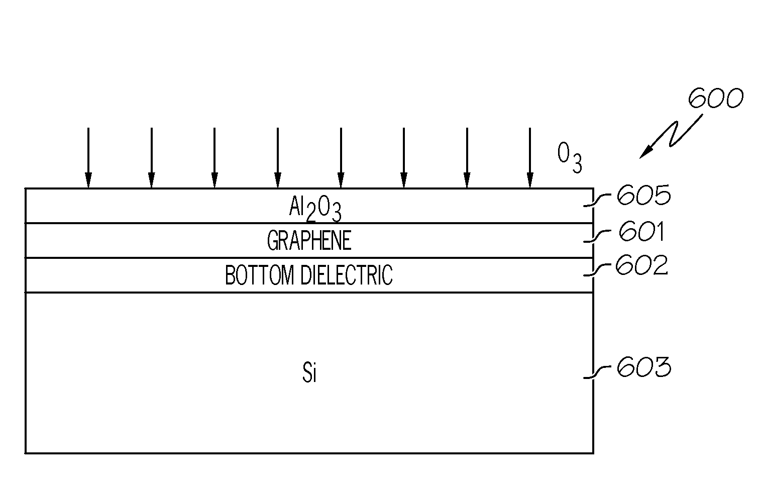
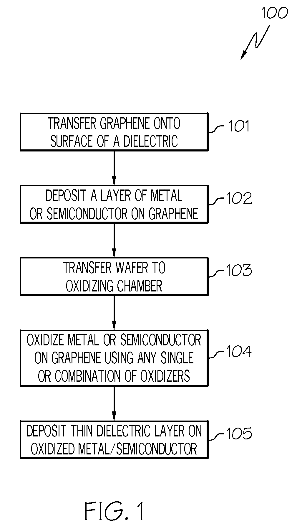
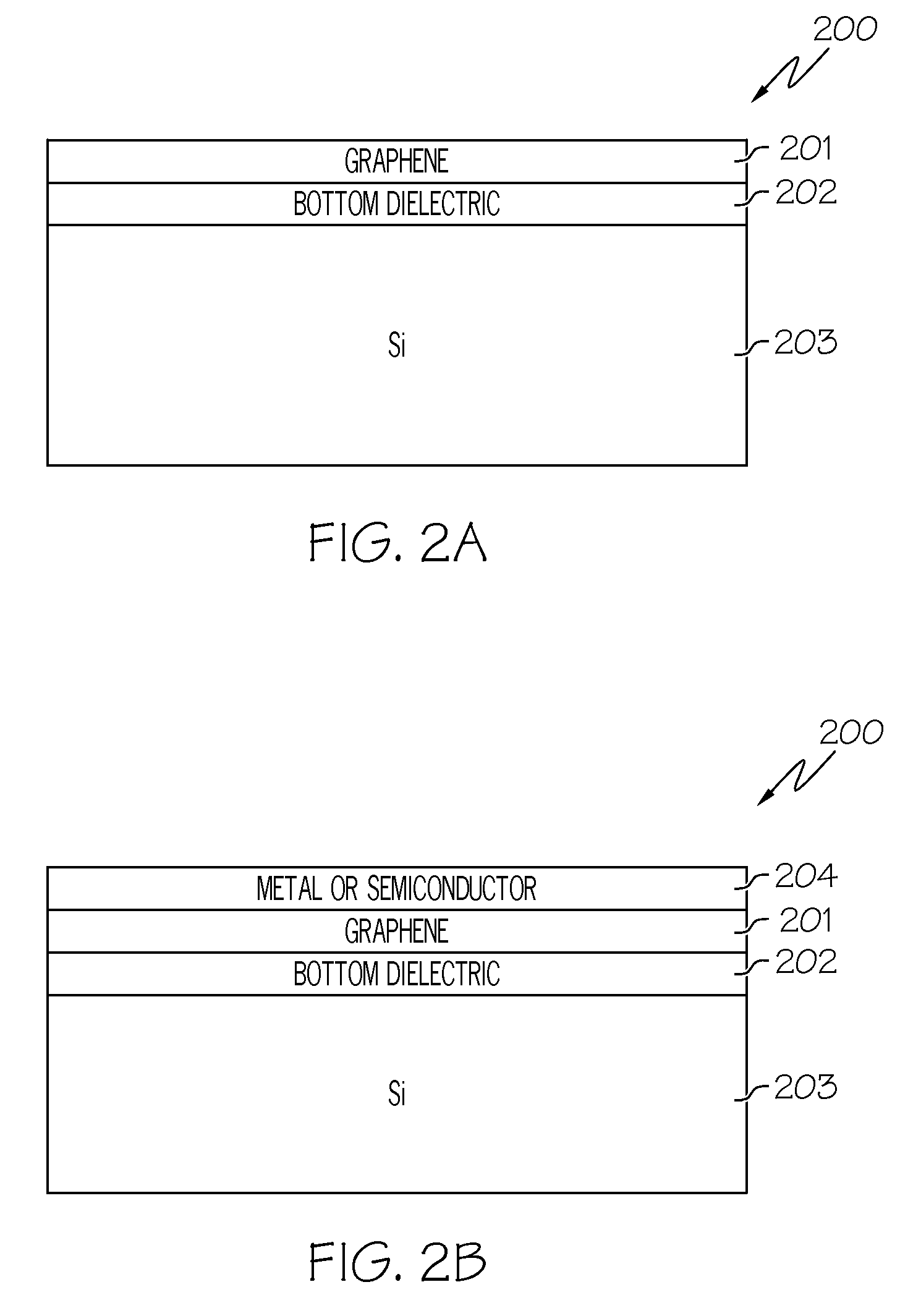
[0019]The present invention comprises a method and semiconductor device for forming a uniformly thin dielectric layer on graphene. In one embodiment of the present invention, a metal or semiconductor layer is deposited on graphene which is transferred to the surface of a dielectric (e.g., silicon dioxide, high-k gate dielectrics) or transferred to the surface of a substrate (e.g., silicon carbide). The metal or semiconductor layer may act as a nucleation layer for graphene thereby allowing a thin dielectric layer to be formed on the graphene after the dielectric layer is deposited on the metal or semiconductor layer. Furthermore, the metal or semiconductor layer may be subjected to an oxidation process. Additionally, the metal or semiconductor layer may be subjected to an ozidizing agent and then subjected to a metal precursor. A dielectric layer may be formed on the graphene after the metal precursor is oxidized. As a result of depositing a metal or semiconductor layer on graphene ...


PUM


Abstract

A method and semiconductor device for forming a uniformly thin dielectric layer on graphene. A metal or semiconductor layer is deposited on graphene which is located on the surface of a dielectric layer or on the surface of a substrate. The metal or semiconductor layer may act as a nucleation layer for graphene. The metal or semiconductor layer may be subjected to an oxidation process. A thin dielectric layer may then be formed on the graphene layer after the metal or semiconductor layer is oxidized. As a result of synthesizing a metal-oxide layer on graphene, which acts as a nucleation layer for the gate dielectric and buffer to graphene, a uniformly thin dielectric layer may be established on graphene without affecting the underlying characteristics of graphene.

Description

TECHNICAL FIELD[0001]The present invention relates to semiconductor device fabrication, and more particularly to establishing a uniformly thin dielectric layer on graphene in a semiconductor device without affecting the properties of graphene.BACKGROUND OF THE INVENTION[0002]A material called graphene has recently been discovered which has the ideal properties believed to make it an excellent component of integrated circuits. Graphene is a one-atom-thick planar sheet of sp2-bonded carbon atoms that are densely packed in a honeycomb crystal lattice. The carbon-carbon bond length in graphene is approximately 1.42 Å. Graphene is the basic structural element of all other graphite materials including graphite, carbon nanotubes and fullerenes.[0003]Graphene has a high carrier mobility as well as low noise thereby allowing it to be utilized as a component in an electronic device. Thin dielectrics, such as gate dielectrics, with a thickness ranging from about one monolayer to about 15 nanom...

Claims


Application Information

Patent Timeline
IPC IPC(8): H01L29/00H01L21/18
CPCH01L21/28255H01L29/513H01L29/51H01L29/1606
Inventor COLOMBO, LUIGIBANERJEE, SANJAYKIM, SEYOUNGTUTUC, EMANUEL
Owner BOARD OF RGT THE UNIV OF TEXAS SYST
Why Eureka
Try Eureka