Regulator Circuit and RFID Tag Including the Same

a technology of rfid tag and rfid circuit, which is applied in the direction of electric variable regulation, process and machine control, instruments, etc., can solve the problems of affecting the operation of the circuit, malfunctioning other circuits in the rfid tag, and extremely sensitive circuits to high-frequency noise from the outside, so as to improve the noise margin improve the reliability of the rfid tag, and improve the noise margin

Inactive Publication Date: 2010-07-22
SEMICON ENERGY LAB CO LTD
View PDF20 Cites 7 Cited by
  • Summary
  • Abstract
  • Description
  • Claims
  • Application Information

AI Technical Summary

Benefits of technology

[0020]By employing the aforementioned structures, a regulator circuit with an improved noise margin is provided. In addition, the use of the regulator circuit results in an improvement in the noise margin of an RFID tag and further an increase in the reliability of the RFID tag in communication.

Problems solved by technology

In such a case, some terminals connected to circuits in the RFID tag cannot be grounded, which can make the circuits extremely sensitive to high-frequency noise from the outside.
Particularly in a regulator circuit for stabilizing a DC potential generated in the RFID tag, the aforementioned high-frequency noise enters a node in the regulator circuit to adversely affect the circuit operation in some cases.
As a result, the potential output from the regulator circuit becomes unstable and varies, leading to malfunction of the other circuits in the RFID tag which operate on the basis of the potential.

Method used


Image

  • Regulator Circuit and RFID Tag Including the Same
  • Regulator Circuit and RFID Tag Including the Same
  • Regulator Circuit and RFID Tag Including the Same

Examples


embodiment 1

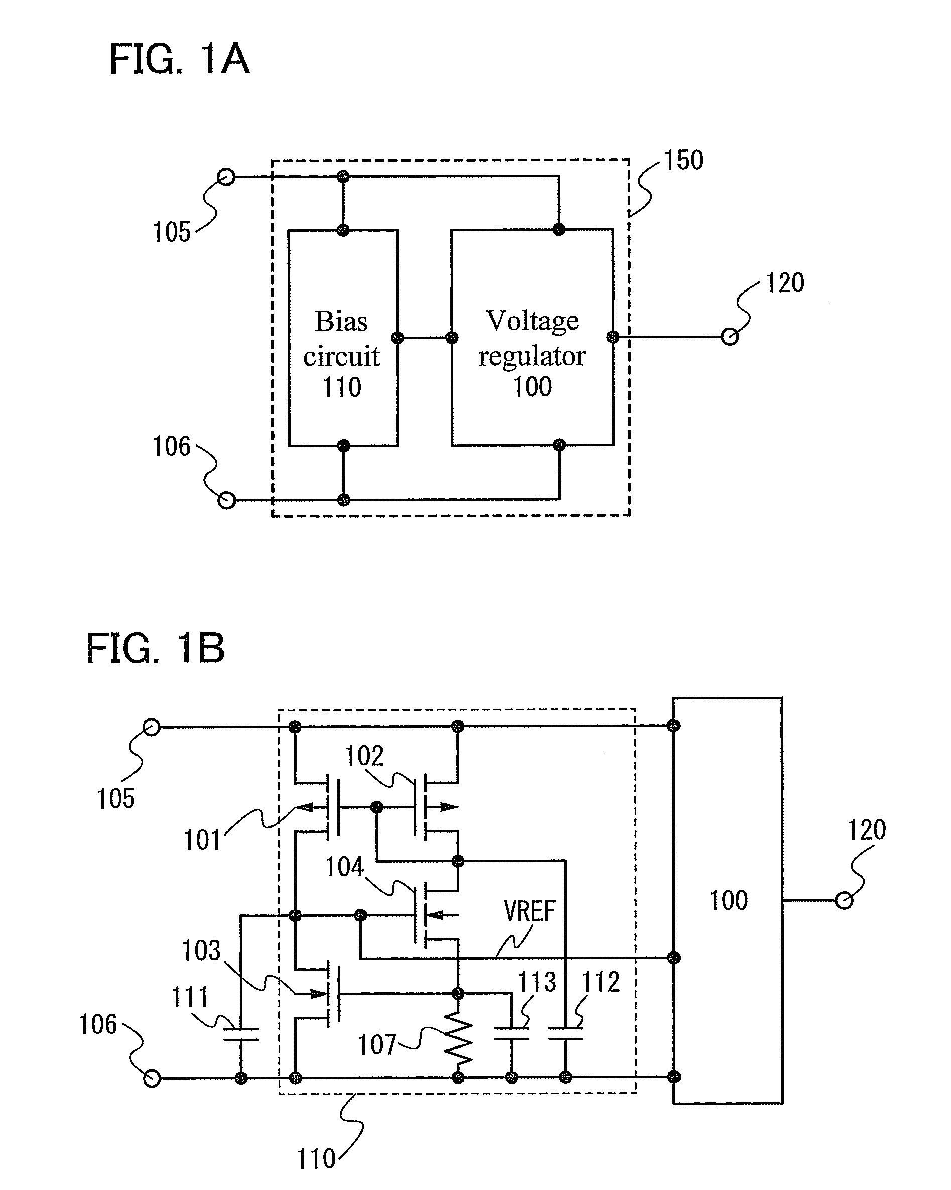
[0033]An example of a configuration of a regulator circuit in this embodiment will be described with reference to FIGS. 1A and 1B.

[0034]As illustrated in FIG. 1A, a regulator circuit 150 disclosed in this embodiment includes a voltage regulator 100 and a bias circuit 110.

[0035]A reference power supply terminal 106 is a terminal to which a potential as a reference of a power supply voltage applied to the circuit illustrated in FIG. 1A is applied. In general, 0 V is applied to the reference power supply terminal 106, though other voltages may also be applied thereto because the potential applied to the reference power supply terminal 106 is only a reference of the power supply voltage of the circuit.

[0036]To an input power supply terminal 105, a potential obtained by using the potential of the reference power supply terminal 106 as a reference is applied.

[0037]The bias circuit 110 generates a potential VREF as a reference potential of the voltage regulator 100 in accordance with a vol...

embodiment 2

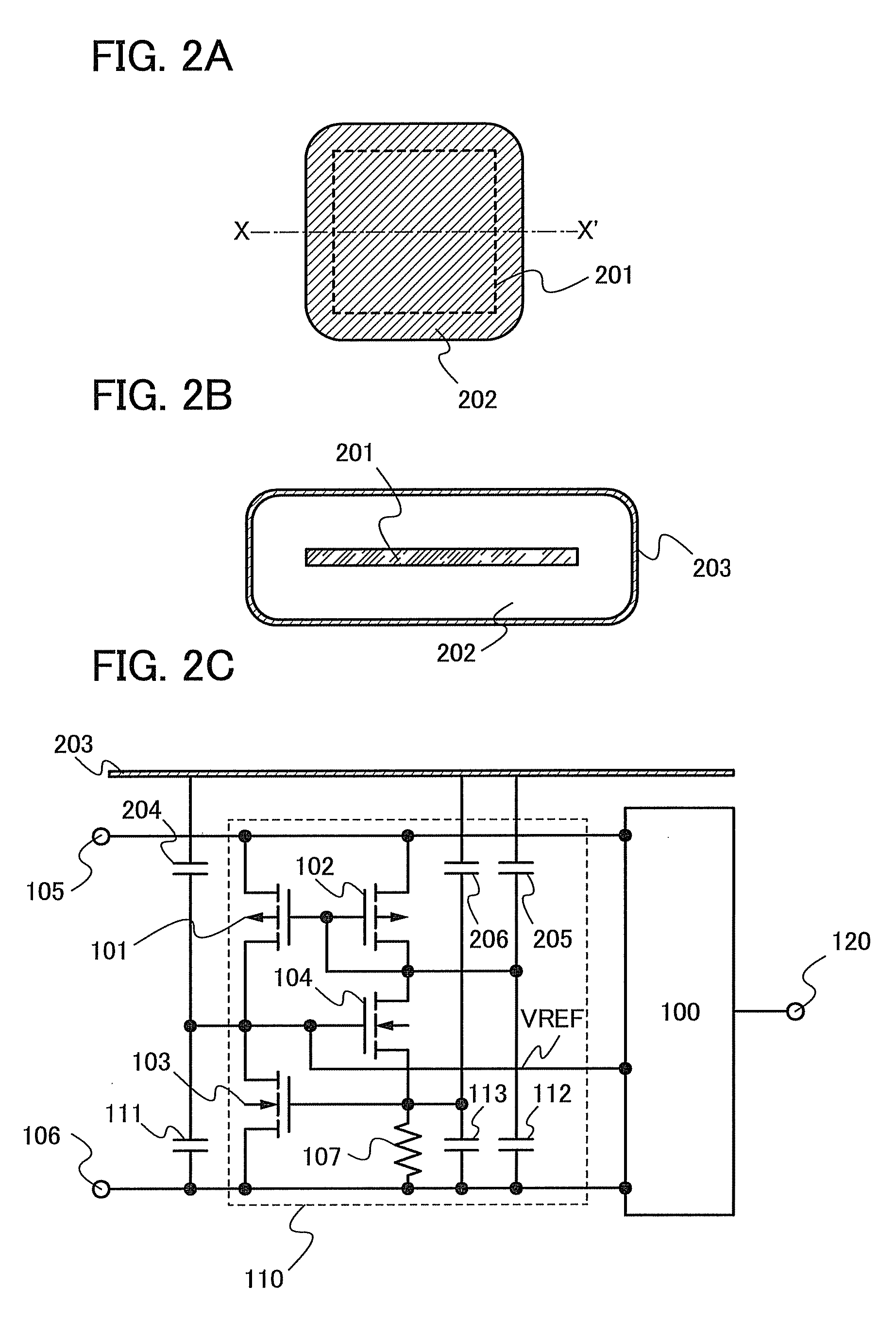
[0059]An RFID tag usually operates without a power supply directly connected thereto because of its application mode. In such a case, some terminals connected to circuits in the RFID tag cannot be grounded, which makes it difficult to take countermeasures against static electricity by utilizing grounding. In this embodiment, an example of countermeasures against static electricity in an RFID tag will be shown.

[0060]FIG. 2A is a top view of an RFID tag. A semiconductor integrated circuit 201 includes a regulator circuit and circuits having a function as an RFID tag, such as a rectifier circuit, a modulation circuit, a demodulation circuit, and other logic circuits. The semiconductor integrated circuit 201 is covered with a support 202. Furthermore, a shield 203 that is a thin film made of a conductive material is provided on the outside of the support, thereby protecting the elements included in the semiconductor integrated circuit 201 against electrostatic discharge.

[0061]FIG. 2B is...

embodiment 3

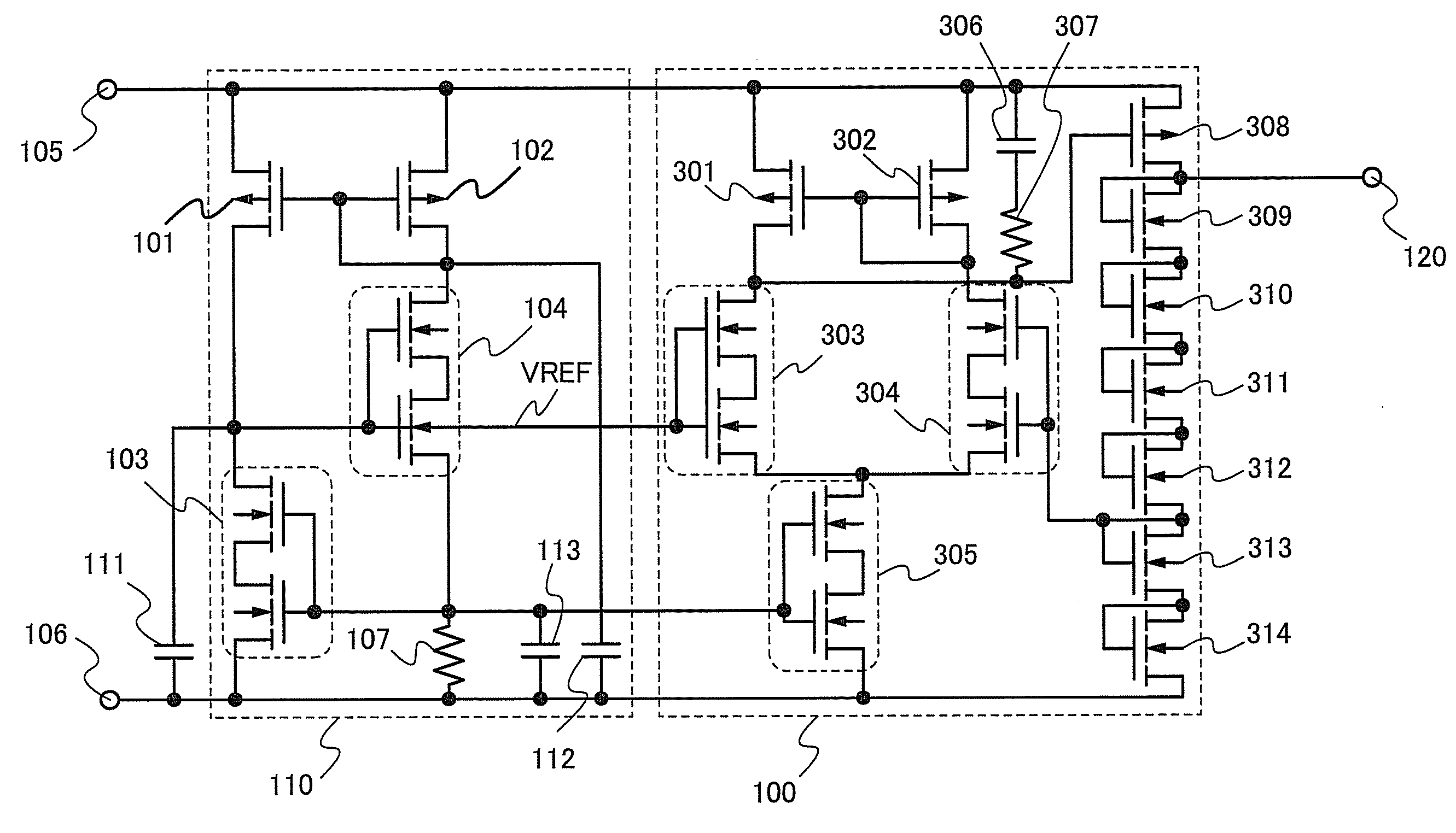
[0068]FIG. 3 illustrates an example of a configuration of the voltage regulator included in the regulator circuit shown in Embodiment 1. The bias circuit 110 has a configuration similar to that described in Embodiment 1. In FIG. 3, double-gate transistors are used as the transistor 103 and the transistor 104; however, single-gate transistors may be used as in Embodiment 1 or multi-gate transistors having three or more gates may also be used.

[0069]The voltage regulator 100 includes a differential amplifier circuit having transistors 301 to 305, a divider circuit having transistors 309 to 314, and an output control transistor that is a p-type transistor 308. The differential amplifier circuit includes a current mirror formed by the transistor 301 and the transistor 302, a differential pair formed by the transistor 303 and the transistor 304, and a current source formed by the transistor 305. A feedback circuit includes the p-type transistor 308 and the divider circuit formed by the n-...


PUM


Abstract

One object of the present invention is to provide a regulator circuit with an improved noise margin. In a regulator circuit including a bias circuit generating a reference voltage on the basis of the potential difference between a first power supply terminal and a second power supply terminal, and a voltage regulator outputting a potential to an output terminal on the basis of a reference potential input from the bias circuit, a bypass capacitor is provided between a power supply terminal and a node to which a gate of a transistor included in the bias circuit is connected.

Description

TECHNICAL FIELD[0001]This specification relates to a regulator circuit with an improved noise margin, and also relates to an RFID tag including the regulator circuit, which transmits and receives data through wireless communication.BACKGROUND ART[0002]In recent years, an environment where the information network is accessible anytime and anywhere has been developed as is called a ubiquitous information society. In such an environment, individual identification technologies have attracted attention. In these technologies, an identification (ID) number is assigned to each object so that the history of the object can be recognized to be utilized in production, management, or the like. Above all, semiconductor devices capable of wirelessly transmitting and receiving data have started to be used.[0003]One of the individual identification technologies having attracted attention utilizes an RFID (radio frequency identification) tag as a semiconductor device that is capable of wirelessly tr...

Claims


Application Information

Patent Timeline
Patent Type & Authority Applications(United States)
IPC IPC(8): G05F3/16
CPCG05F1/56G05F3/16G05F3/242
Inventor INOUE, HIROKIKATO, KIYOSHINAGATSUKA, SHUHEIKAMATA, KOICHIROMURAKAWA, TSUTOMUTUJI, TAKAHIROIKADA, KAORI
Owner SEMICON ENERGY LAB CO LTD
Why Eureka
Try Eureka