Semiconductor memory device and read wait time adjustment method thereof, memory system, and semiconductor device

a semiconductor memory device and read wait time technology, applied in the direction of information storage, static storage, digital storage, etc., can solve the problem that the data read speed of the semiconductor memory device itself is not increased so much

Inactive Publication Date: 2010-07-22
LONGITUDE LICENSING LTD
View PDF6 Cites 24 Cited by
  • Summary
  • Abstract
  • Description
  • Claims
  • Application Information

AI Technical Summary

Benefits of technology

[0046]In the semiconductor memory device according to the present invention, which operates in synchronization with the system clock supplied from the outside and outputs read data, and in the memory system according to the present invention that uses the semiconductor memory devices, even if the synchronous circuit such as a DLL or a PLL is not used, an access time substantially equal to that achieved through the use of the synchronous circuit can be ensured.
[0047]Further, in the semiconductor device according to the present invention, which operates in synchronization with the system clock supplied from the outside and outputs data, even if the synchronous circuit such as the DLL or PLL is not used, an access time comparable to that achieved through the use of the synchronous circuit can be ensured.

Problems solved by technology

However, when the DLL-off mode is actually used, the problem that will be described below arises.
However, the data read speed of the semiconductor memory device itself is not increased so much.

Method used


Image

  • Semiconductor memory device and read wait time adjustment method thereof, memory system, and semiconductor device
  • Semiconductor memory device and read wait time adjustment method thereof, memory system, and semiconductor device
  • Semiconductor memory device and read wait time adjustment method thereof, memory system, and semiconductor device

Examples


first example

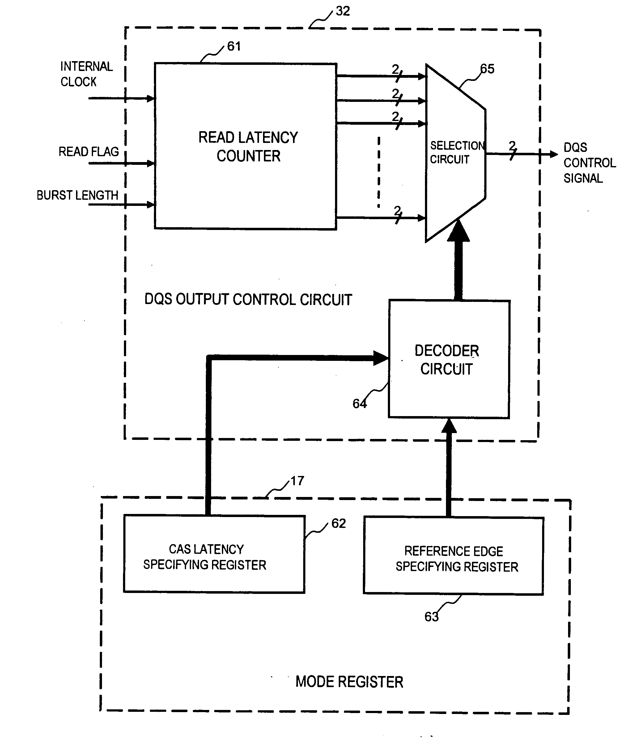
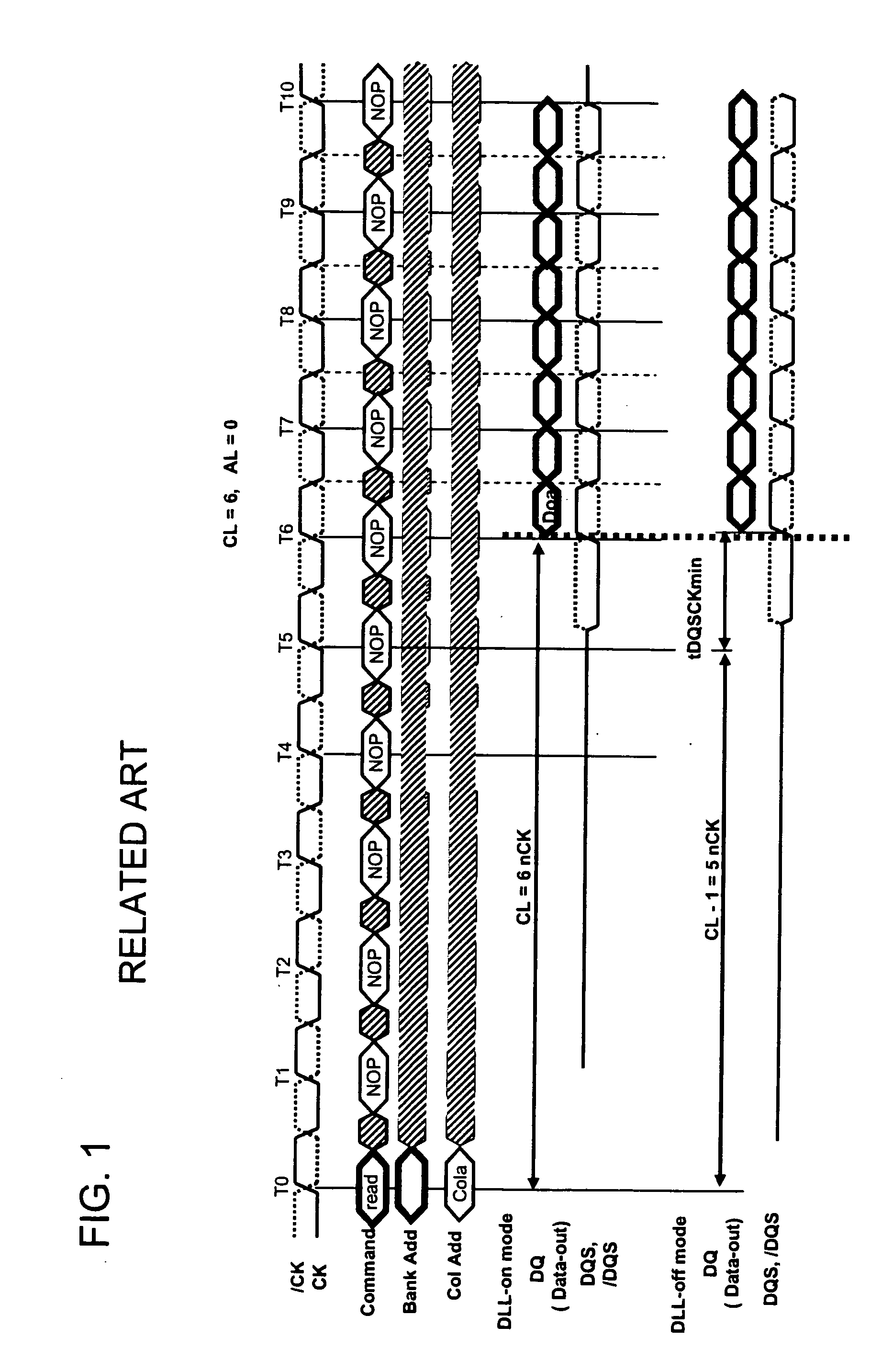
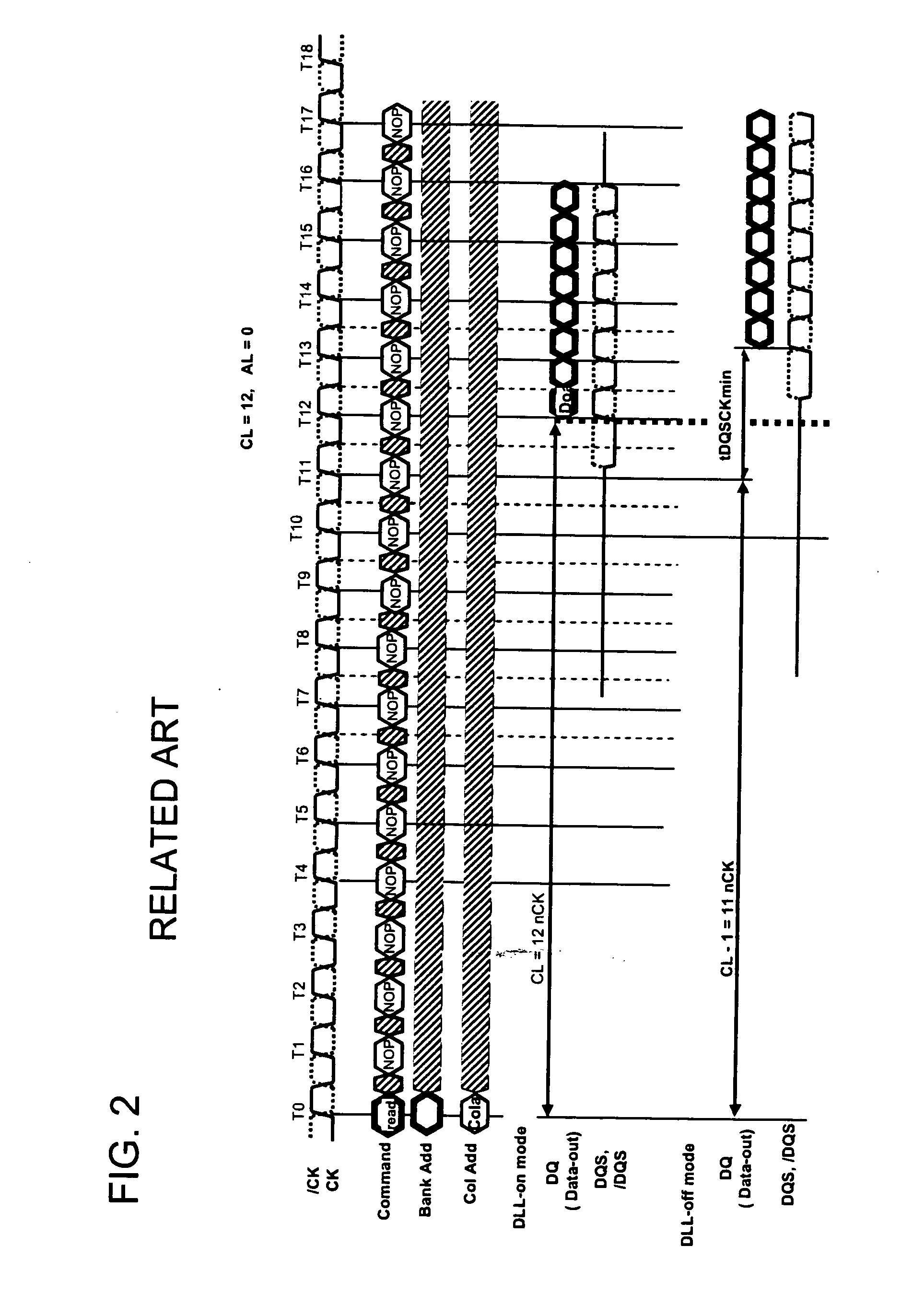
[0074]FIG. 3 is a configuration diagram of an overall memory system in an example of the present invention. FIG. 3 is the memory system for reading and writing of 64 bits in parallel. A semiconductor memory device 1 is used for reading and writing of eight bits in parallel. Eight semiconductor memory devices 1 are connected in parallel to perform reading and writing of 64 bits in parallel. In the memory system in FIG. 3, a configuration is assumed in which two ranks of the semiconductor memory devices 1 of are respectively mounted on two DIMMs (Dual Inline Memory Modules). That is, the memory system is formed of the semiconductor memory devices of a total of four ranks which are indicated by DIMM1 Rank-1, DIMM1 Rank-2, DIMM2 Rank-1, and DIMM2 Rank-2. Each rank is further formed of the eight semiconductor memory devices 1. A total of 4 ranks*8=32 semiconductor memory devices 1 are mounted. FIG. 3 illustrates only three of the eight semiconductor memory devices 1 connected in parallel...


PUM


Abstract

A semiconductor memory device operates in synchronization with a system clock, without using a synchronous circuit such as a DLL or a PLL. The semiconductor memory device includes a synchronous circuit for generating output signals phase aligned with the system clock, a synchronous circuit selection circuit that performs switching between a synchronous circuit selection mode and a synchronous circuit non-selection mode, and a reference edge specifying register that specifies an edge of an internal clock which serves as a reference for outputting read data in the synchronous circuit non-selection mode. In the synchronous circuit selection mode, the read data is output by adjusting a phase deviation of the internal clock with respect to the system clock, using the synchronous circuit. In the synchronous circuit non-selection mode, the read data is output in synchronization with the internal clock, without using the synchronous circuit. For a delay of the internal clock with respect to the system clock, the edge of the internal clock used as the reference is adjusted by the reference edge specifying register. Then, even if the synchronous circuit is not used, a large timing deviation does not thereby occur.

Description

TECHNICAL FIELD[0001]1. Reference to Related Application[0002]This application is based upon and claims the benefit of the priority of Japanese patent application No. 2009-007829, filed on Jan. 16, 2009, the disclosure of which is incorporated herein in its entirety by reference thereto.[0003]The present invention relates to a semiconductor memory device and a read wait time adjustment method thereof, a memory system, and a semiconductor device. More specifically, the invention relates to an operation when a synchronous circuit such as a PLL or a DLL is not used in a semiconductor memory device or a semiconductor device that operates in synchronization with a system clock.[0004]2. Background[0005]There have been remarkable increases in capacity and speed of semiconductor memory devices including a dynamic RAM. In a DDR SDRAM (Double Data Rate Synchronous DRAM) in particular, internal operations are pipelined, and commands that have been supplied from an outside in synchronization wi...

Claims


Application Information

Patent Timeline
Patent Type & Authority Applications(United States)
IPC IPC(8): G11C7/00G11C8/18
CPCG11C7/1051G11C7/1066G11C7/1072G11C7/22G11C7/222G11C11/4076G11C11/4096G11C8/18
Inventor KOSHIZUKA, ATSUO
Owner LONGITUDE LICENSING LTD
Why Eureka
Try Eureka