Digital to time converter and digital to time converting method
a digital to time converter and digital to time conversion technology, applied in the field of can solve the problems of poor linearity insatiable corresponding accuracy, and easy affecting performance of conventional digital to time converters
- Summary
- Abstract
- Description
- Claims
- Application Information
AI Technical Summary
Problems solved by technology
Method used
Image


Examples
first embodiment
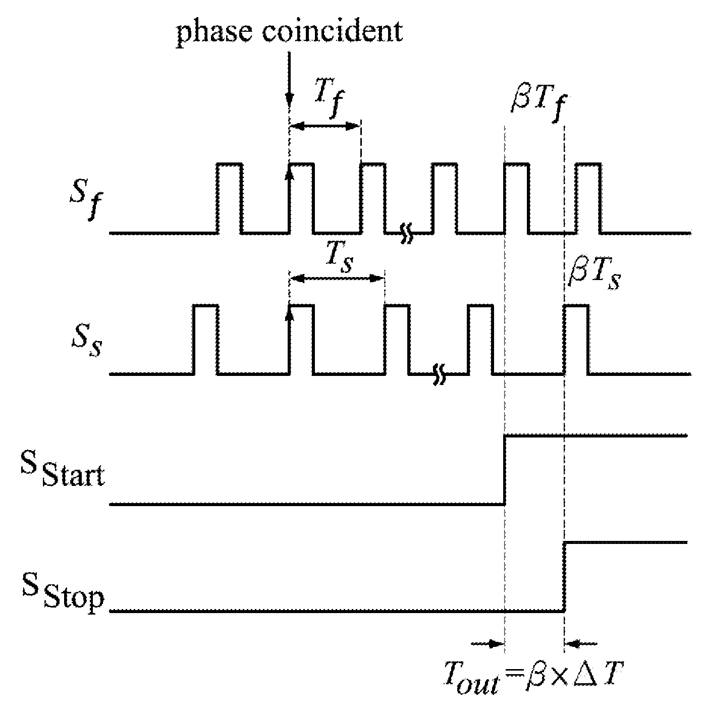
[0028]FIG. 2 is a schematic diagram showing a digital to time converter according to the invention. The digital to time converter 100 comprises periodic signal generators 101 and 102, a periodic signal synchronizer 103 and output pulse generators 104 and 105. The periodic signal generators 101 and 102 generate a periodic signal SF with a period TF and a periodic signal SS with a period TS respectively, wherein the period TS is longer than the period TF and the difference between the periods TS and TF is ΔT. According to an embodiment of the invention, the periodic signal generators 101 and 102 may be the oscillators to generate the periodic signals SF and SS with corresponding frequencies 1 / TF and 1 / TS. The periodic signal synchronizer 103 is coupled to the periodic signal generators 101 and 102 and comprises a phase detector 201 detecting the phase difference between the periodic signals SF and SS and outputting a phase indication signal SPD. Each of the output pulse generators 104...
second embodiment
[0032]FIG. 5 illustrates a schematic diagram of a typical phase-locked loop according to the invention. The phase-locked loop 500 comprises a phase detector 501, a charge pump 502, a low pass filter (LPF) 503, a voltage controlled oscillator (VCO) 504 and a divider (or called a prescaler) 505. Assumes a divisor of the divider is M, then the relationship between the frequencies of an output signal So and the reference signal Sref is derived as:
fo=Mfref Eq.(5),
and the period may be expressed as:
To=Tref / M Eq. (6).
Eq.(6) shows that the period Tref of the reference signal Sref is a multiple of the period To of the output signal So. Thus, after oscillating for M times, a rising edge of the output signal So naturally and perfectly coincides with a rising edge of the reference signal Sref.
[0033]Based on the concept, and referring back to FIG. 4, when two PLLs are used as the periodic signal generators 401 and 402 and the output signals of the VCOs of the PLLs are further used as the out...
third embodiment
[0038]FIG. 9 is a circuit diagram illustrating the coupling between the VCO of the PLL and the multiplexer according to the invention. As shown in FIG. 9, the VCO 504 may comprise a series of delay units for generating a plurality of oscillation signals SF,φ0˜SF,φK-1 with different phases according to a predetermined phase offset. Thus, the PLL may further provide K oscillation signals with K different phases. Referring back to FIG. 8, if both of the periodic signal generators 801 and 802 generate signals with K different phases, the phase difference between the two output periodic signals may be 1 / K times of ΔT. In this way, a finest resolution may be obtained as:
ΔP=ΔTK=(TrefM-TrefN)K.Eq.(9)
[0039]Thus, by using one more set of switches or a multiplexer coupled to the VCO as shown in FIG. 9 for selecting a specific output phase, the predetermined time delay Tout becomes:
Tout=(α+β)×TS−β×TF+γS×ΔPS−γF×ΔPF Eq.(10)
, wherein γF represents a selection value for controlling the switches o...
PUM
 Abstract
Description
Claims
Application Information
 - R&D
- Intellectual Property
- Life Sciences
- Materials
- Tech Scout
- Unparalleled Data Quality
- Higher Quality Content
- 60% Fewer Hallucinations
Browse by: Latest US Patents, China's latest patents, Technical Efficacy Thesaurus, Application Domain, Technology Topic, Popular Technical Reports.
© 2025 PatSnap. All rights reserved.Legal|Privacy policy|Modern Slavery Act Transparency Statement|Sitemap|About US| Contact US: help@patsnap.com