Epitaxial methods and structures for forming semiconductor materials

a technology of semiconductor materials and substrates, applied in the direction of semiconductor devices, basic electric elements, electrical apparatus, etc., can solve the problems that random arrangement of islands of high quality materials is not practical useful for the formation of substrates or device structures

Inactive Publication Date: 2010-07-29
SOITEC SA
View PDF17 Cites 18 Cited by
  • Summary
  • Abstract
  • Description
  • Claims
  • Application Information

AI Technical Summary

Benefits of technology

[0011]The embodiments of the invention are concerned with the formation of substantially continuous films of semiconductor material (e.g., III-nitrides) which have improved material characteristics, namely a reduced density of defects / dislocation, substantially strain-relaxed (i.e., reduced levels of lattice strain) and substantially free of phase separation (e.g., an InGaN material of a single composition).
[0018]To prevent strain relaxation in the lateral growth regions, the thickness of the regions is maintained at or below the critical thickness, and, as a result, the lateral growth regions are strained and maintain the in-plane lattice parameter of the high quality island structures, whilst preventing the formation of additional defects / dislocation by preventing strain relaxation.

Problems solved by technology

However, separate randomly arranged island structures of high quality material are not practically useful for the formation of substrates or device structures etc., due to their random nature and small dimensions.

Method used


Image

  • Epitaxial methods and structures for forming semiconductor materials
  • Epitaxial methods and structures for forming semiconductor materials
  • Epitaxial methods and structures for forming semiconductor materials

Examples


examples

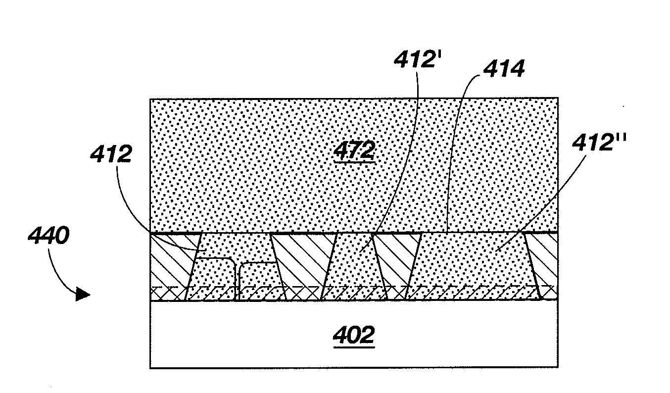
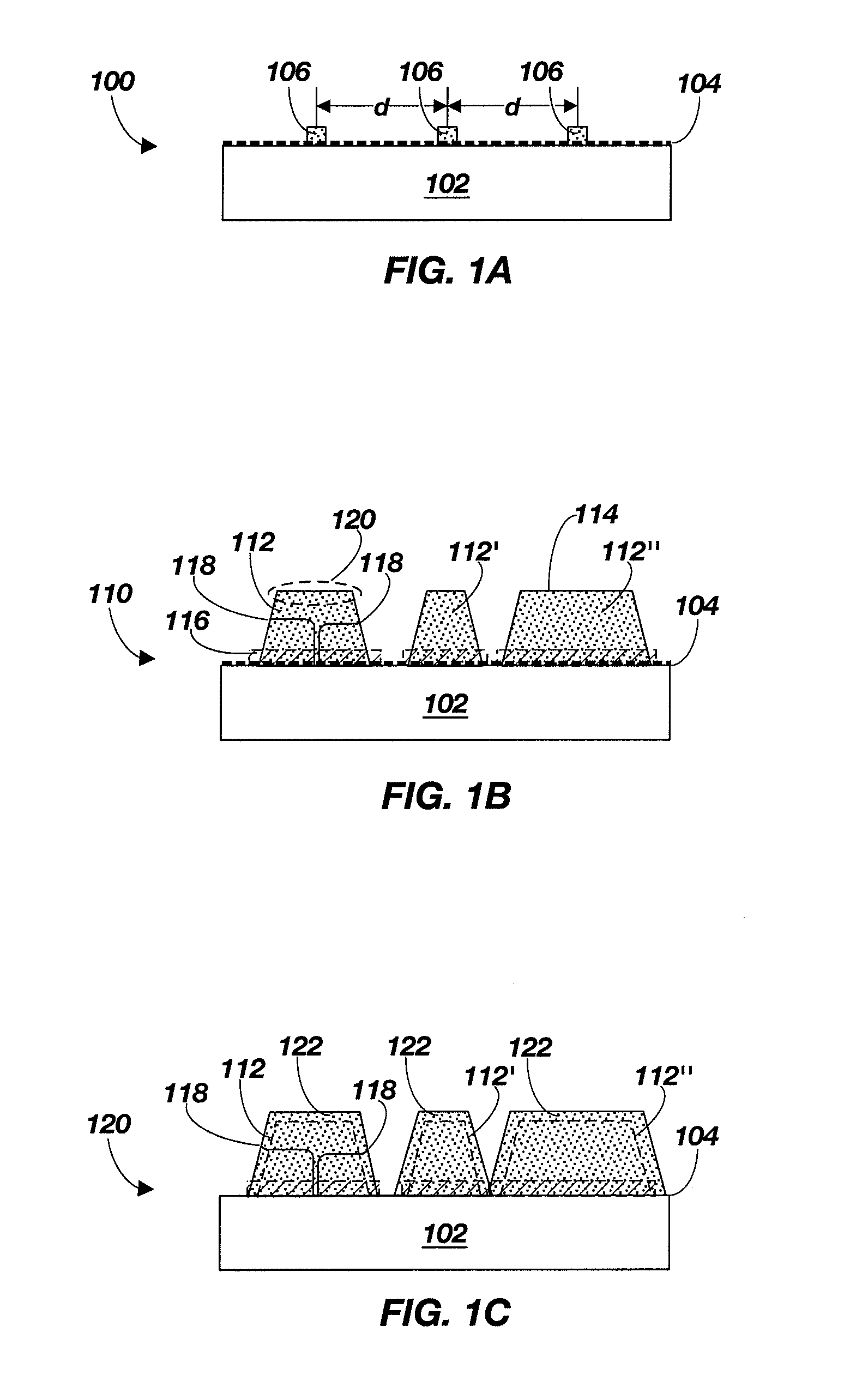
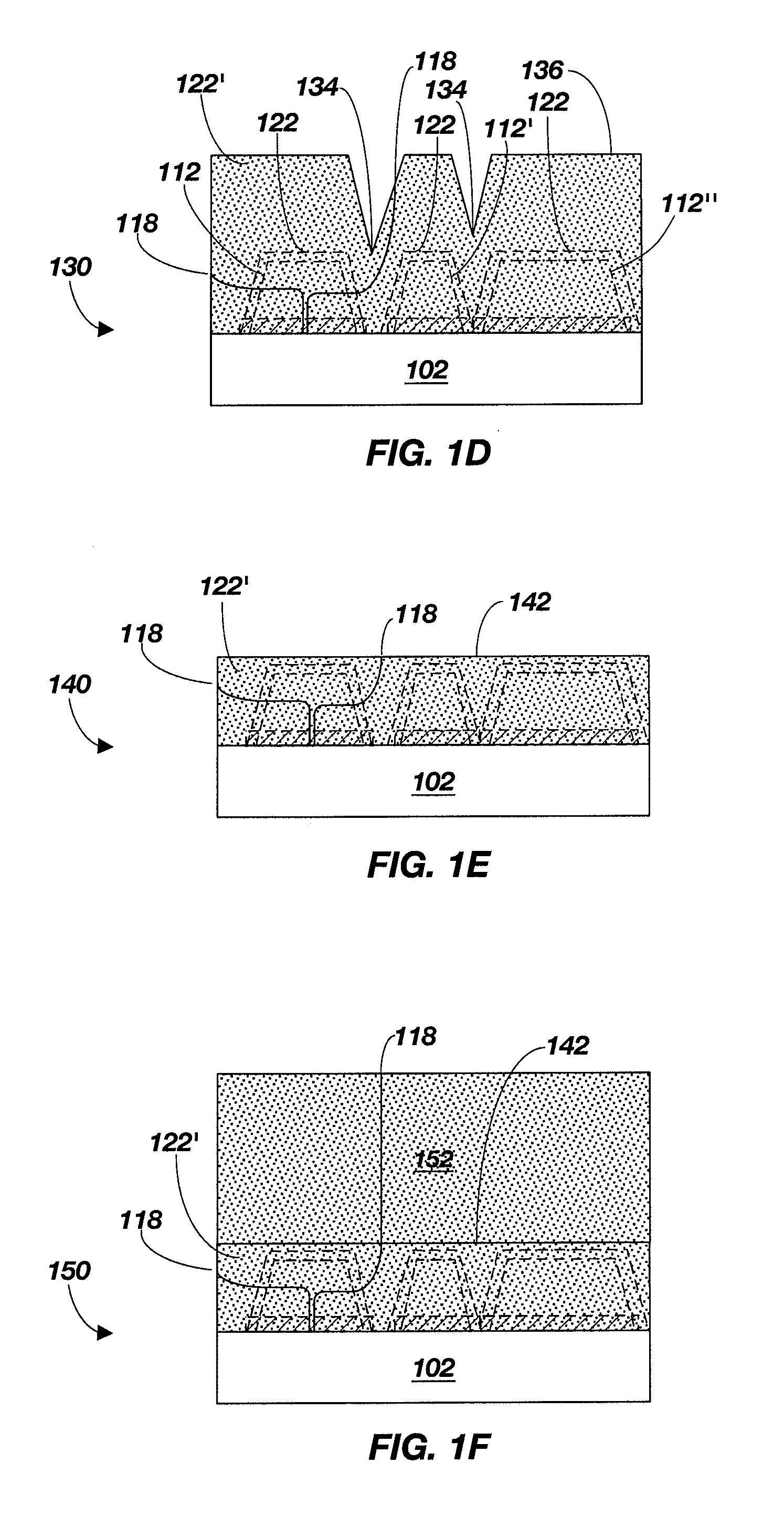
[0142]FIG. 5 illustrates a scanning electron microscopy (SEM) top view image and FIG. 6A-B illustrate transmission electron microscopy (TEM) side view images of actual examples of InGaN island structures formed on base substrates utilizing embodiments of the invention previously outlined. In particular, island structures 612, 612′ and 612″ (of FIG. 6A) correspond to those illustrated in the intermediate structure 110 in FIG. 1B. In addition, FIG. 6C illustrates a substantially continuous layer of strain-relaxed InGaN produced using embodiments of the invention.

[0143]The island structures of FIGS. 5 and 6A-B have been produced by the following means. Prior to deposition of the InGaN island structures, a sapphire substrate is heated within a MOVPE reactor to a temperature of between 600-900° C. In certain embodiments, the temperature is maintained at 750° C. whilst ammonia is introduced into the reaction chamber for 3-5 mins to enable the nitridation of the sapphire surface. Subsequen...


PUM

PropertyMeasurementUnit
distanceaaaaaaaaaa
vertical/lateral aspect ratioaaaaaaaaaa
aspect ratioaaaaaaaaaa

Abstract

Methods and structures for producing semiconductor materials, substrates and devices with improved characteristics are disclosed. Structures and methods for forming reduced strain structures include forming a plurality of substantially strain-relaxed island structures and utilizing such island structures for subsequent further growth of strain-relaxed substantial continuous layers of semiconductor material.

Description

CROSS-REFERENCE TO RELATED APPLICATION[0001]This application claims benefit under 35 U.S.C. §119(e) of U.S. Provisional Application No. 61 / 147,881 filed Jan. 28, 2009, which is incorporated herein by reference.FIELD OF THE INVENTION[0002]The various embodiments of the present invention generally relate to the fabrication of semiconductor structures and substrates. The various embodiments provide methods and structures for producing semiconductor materials and substrates with improved characteristics.BACKGROUND OF THE INVENTION[0003]Strained layers of semiconductor materials can be undesirable for a number of reasons. Strain in the semiconductor layers can result in an increased density of defects, crack formation and phase separation, in broad terms, a possible reduction in material quality.[0004]Strain effects can be disadvantageous in fabricating III-V semiconductor materials such as the III-nitrides. For example, consider III-nitride based light emitting devices containing indium...

Claims


Application Information

Patent Timeline
Patent Type & Authority Applications(United States)
IPC IPC(8): H01L29/20H01L21/20
CPCH01L21/0242H01L21/02458H01L21/0254H01L29/2003H01L21/02639H01L21/02647H01L21/0265H01L21/0262
Inventor ARENA, CHANTAL
Owner SOITEC SA
Why Eureka
Try Eureka