Imaging lens, imaging device, and mobile terminal

a technology of imaging device and lens, applied in the field of imaging lens, can solve the problems of reducing diffraction efficiency in wavelengths other than design wavelengths, difficult to form diffracting surface and refracting interface simultaneously on the lens flat plate, etc., to achieve miniaturization and mass production capability, reduce the amount of sag on the surface, and reduce the effect of error sensitivity that heavily depends on the position of the diaphragm

Inactive Publication Date: 2010-07-29
KONICA MINOLTA OPTO
View PDF21 Cites 47 Cited by
  • Summary
  • Abstract
  • Description
  • Claims
  • Application Information

AI Technical Summary

Benefits of technology

[0082]According to the present invention, the incidence angle of the peripheral light ray with respect to a lens element formed on the image-side surface of the i-th flat plate is kept small by forming a convex shape directed to the object-side on a lens element formed on an object-side surface of an i-th flat plane lens at the most distant position (in the vicinity of the optical path, which is most distant from the optical axis, of the light ray emitted from an object) from the optical axis. Thereby, a lens element formed on the image-side surface of the i-th lens flat plate does not need to control the incidence angle with respect to a solid-state image sensing device small. Therefore, aspheric surface sag amount is reduced. Thus, the lens element on the i-th lens flat plate can be thin, and a miniaturization of the whole imaging lens can be attained. A conditional relationship (A) specifies a distance on the optical axis (distance between lenses) between the (i−1)th lens and the i-th lens. In order to satisfy the conditional relationship (A), the (i−1)th lens is put closer to the image side as much as possible, and the (i−1)th lens thus works as a negative lens in order to maintain the telecentricity of the light ray at the maximum view angle. As a result, a lens element of the first lens can be made thin.
[0083]In the present invention, the error sensitivity that heavily depends on a diaphragm position can be moderated by placing the diaphragm the more image-side than the most object-side lens peak, in other words, by placing the lens or a lens element on the most object-side. The error sensitivity will become critical when arranging three or more lenses in a compact formation. By placing the diaphragm according to this arrangement, miniaturization and mass production capability are both possible.
[0084]In the present invention, the curvature of field in the peripheral portion can be satisfactorily corrected by making surface convex toward the image side at a position where the principal ray of the maximum image height passes through the (i−1)th lens. Therefore, the burden of aberration correction of the i-th lens can be reduced. Thus, it becomes possible to make the lens element of the i-th lens thin.
[0085]The conditional relationship (1) in the present invention specifies the focal length of the object-side surface of the first lens. A satisfactory aberration performance and a short overall optical length can be obtained by satisfying the conditional relationship (1).

Problems solved by technology

However, there is a technical limitation to achieving both of further microminiaturization of these optical systems and a mass-production capability required for use in a personal digital assistant.
However, it is not easy to form a diffracting surface and a refracting interface simultaneously on a lens flat plate.
There are problems, in use of diffracting surface, that the diffraction efficiency decreases in wavelengths other than a design wavelength and that there is a large restriction to the angle of the incident light entering into the diffracting surface due to the poor angle characteristic of the incident light to the diffracting surface.
Thus, there is a problem of difficulty in securing a wide field angle.
In an optical system given in a patent reference No. 1, although the thickness of a lens element is not thick, there is a problem of a large astigmatism.
In this technique, in the case where the thickness of UV hardening type resin section is approximately greater than 0.25 (mm), there is a problem that a penetration of ultraviolet rays is poor and UV hardening type resin cannot be hardened sufficiently.

Method used


Image

  • Imaging lens, imaging device, and mobile terminal
  • Imaging lens, imaging device, and mobile terminal
  • Imaging lens, imaging device, and mobile terminal

Examples


first embodiment

of the Present Invention

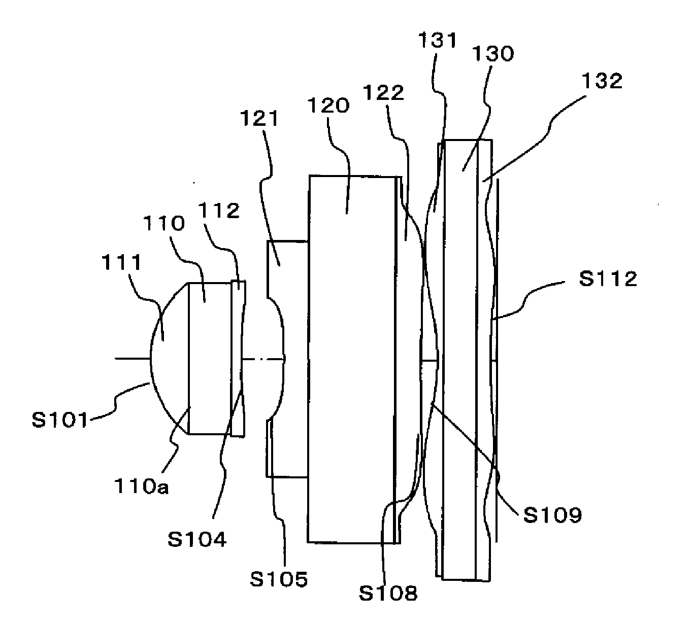
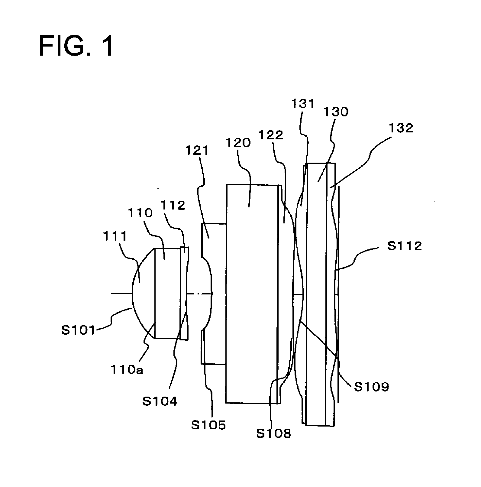
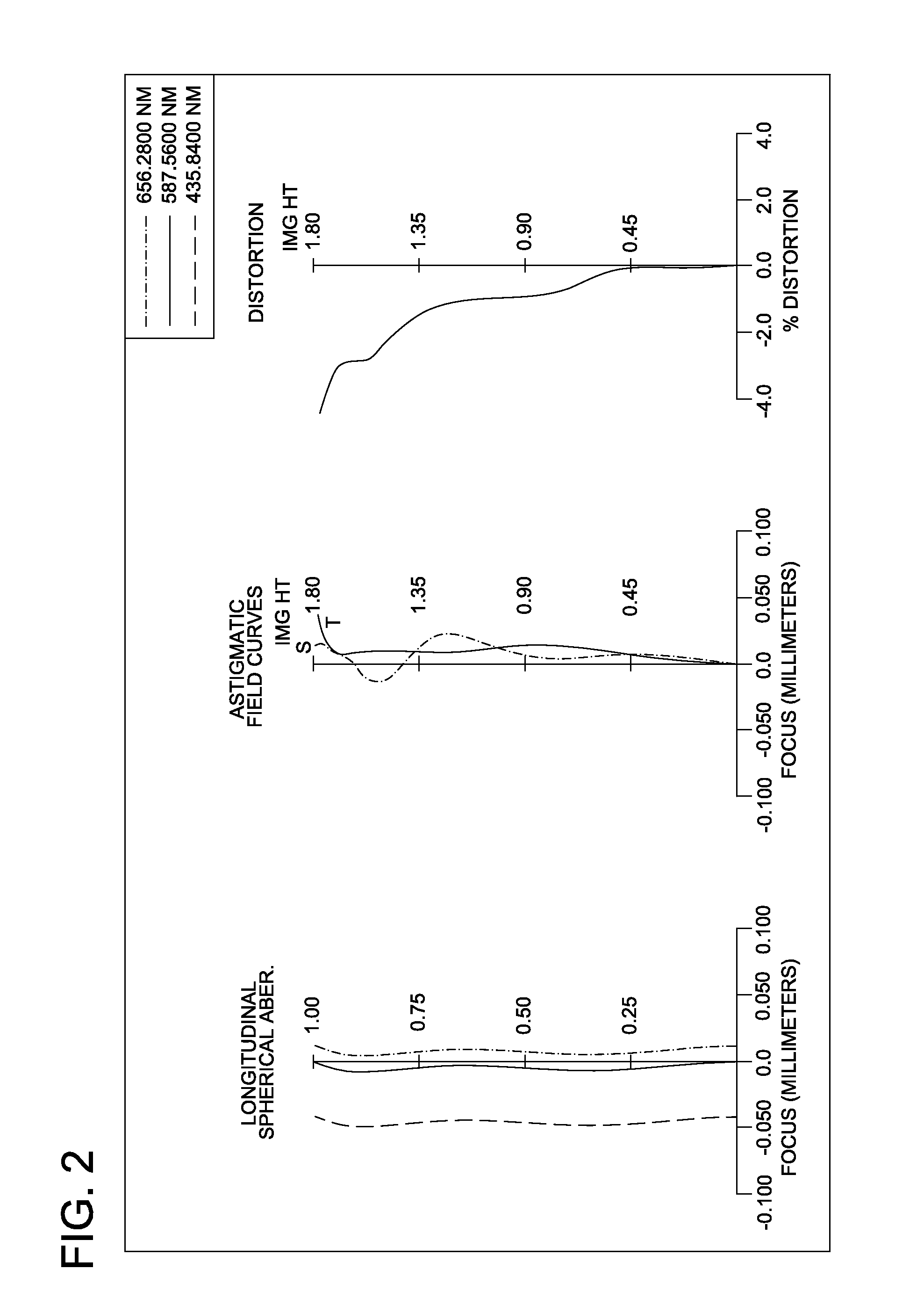
[0135]Hereinafter, an imaging lens according to a first embodiment of the present invention will be described. FIG. 1 illustrates a sectional view of the imaging lens according to this embodiment of the present invention.

[0136]As illustrated in FIG. 1, the imaging lens according to this embodiment of the present invention is configured of a lens system including a 1f-th lens element 111, an aperture diaphragm 110a, a first lens flat plate 110, a 1b-th lens element 112, a 2f-th lens element 121, a second lens flat plate 120, a 2b-th lens element 122, a 3f-th lens element 131, a third lens flat plate 130 and a 3b-th lens element 132 in the order from the object side. Here, the imaging lens configured of three lenses is described in this embodiment. However, the imaging lens may be configured of more lenses. For example, in the case where “i” (i>=4) number of lenses are used, an i-th lens disposed at the most image side may be configured similar to the third len...

second embodiment

[0143]FIG. 3 illustrates a sectional view of the imaging lens according to an second embodiment of the present invention.

[0144]As illustrated in FIG. 3, the imaging lens according to this embodiment of the present invention is configured of a lens system including a 1f-th lens element 211, an aperture diaphragm 210a, a first lens flat plate 210, a 1b-th lens element 212, a 2f-th lens element 221, a second lens flat plate 220, a 2b-th lens element 222, a 3f-th lens element 231, a third lens flat plate 230 and a 3b-th lens element 232 in the order from the object side. Here, the imaging lens configured of three lenses is described in this embodiment. However, the imaging lens may be configured of more lenses. For example, in the case where “i” number of lenses are used, an i-th lens disposed at the most image side may be configured similar to the third lens in this embodiment. In this case, any kind of lens (for example, a bonded lens, a spherical lens or an aspherical lens) may be us...

third embodiment

[0150]FIG. 5 illustrates a sectional view of the imaging lens according to a third embodiment of the present invention.

[0151]As illustrated in FIG. 5, the imaging lens according to this embodiment of the present invention is configured of a lens system including a 1f-th lens element 311, an aperture diaphragm 310a, a first lens flat plate 310, a 1b-th lens element 312, a 2f-th lens element 321, a second lens flat plate 320, a 2b-th lens element 322, a 3f-th lens element 331, a third lens flat plate 330 and a 3b-th lens element 332 in the order from the object side. Here, the imaging lens configured of three lenses is described in this embodiment. However, the imaging lens may be configured of more lenses. For example, in the case where “i” (i>=4) number of lenses are used, an i-th lens disposed at the most image side may be configured similar to the third lens in this embodiment. In this case, any kind of lens (for example, a bonded lens, a spherical lens or an aspherical lens) may ...


PUM


Abstract

Provided are a wafer scale lens, which is so short in an optical total length with respect to an image height that it can correct an aberration satisfactory, and an optical system including the wafer scale lens and having a thin lens element on the side closest to the image. The optical system includes a first lens having a positive refractive power relative to an object, and a second lens arranged on the side of the image of the first lens and having a recessed shape on the side of the object. At least one lens is arranged on the side of the second lens. When that one of the lenses arranged on the side of the image of the second lens, which is arranged on the side closest to the image, is an i-th lens (i>3), this i-th lens includes an i-th lens flat plate and is formed on the object side of the i-th lens flat plate but has a refractive index different from that of the i-th lens flat plate, and a lens element having a convex shape on the object side where the main light ray of the maximum image height passes. Moreover, the ratio between the optical axial distance (or the lens distance) between a (i−1)-th lens and the i-th lens and the optical axis distance (or the optical total length) from the object side face of the first lens to the image face is 0.01 to 0.15.

Description

TECHNICAL FIELD[0001]The present invention relates to an imaging lens for photographing a subject, and an imaging lens of an imaging device using solid-state image sensing devices such as a CCD image sensor and a CMOS image sensor. In detail, the present invention relates to an image imaging lens in an optical system using a wafer-scale lens that is suitable for mass production and an imaging device using the imaging lens.BACKGROUND ART[0002]Small and thin imaging devices have come to be installed in personal digital assistants, which are small-sized and thin electronic equipment, such as a portable telephone and a PDA (Personal Digital Assistant). Whereby, it is possible to mutually transmit not only voice information but also image information to a remote place.[0003]With respect to an image sensor used for such an imaging device, solid-state image sensing devices, such as a CCD (Charge Coupled Device) image sensor and a CMOS (Complementary Metal-Oxide Semiconductor) image sensor,...

Claims


Application Information

Patent Timeline
Patent Type & Authority Applications(United States)
IPC IPC(8): G02B13/18H04N5/225G02B3/00G02B11/08
CPCG02B13/0035G02B13/0085G02B13/006G02B13/004G02B13/18G02B13/00G02B9/00H04N23/00
Inventor HIRAO, YUSUKEMATSUSAKA, KEIJIFUKUTA, YASUNARI
Owner KONICA MINOLTA OPTO
Why Eureka
Try Eureka