

Memory having negative voltage write assist circuit and method therefor
a technology of write assist circuit and memory, which is applied in the field of memory, can solve the problems of difficult to write to memory cells, and difficult to write to array cells
- Summary
- Abstract
- Description
- Claims
- Application Information
AI Technical Summary
Problems solved by technology
Method used
Image

Examples
Embodiment Construction
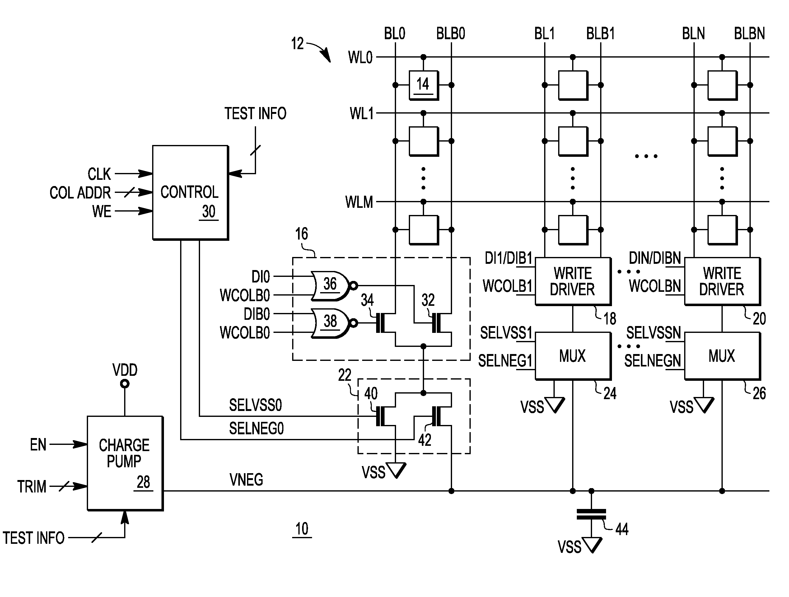
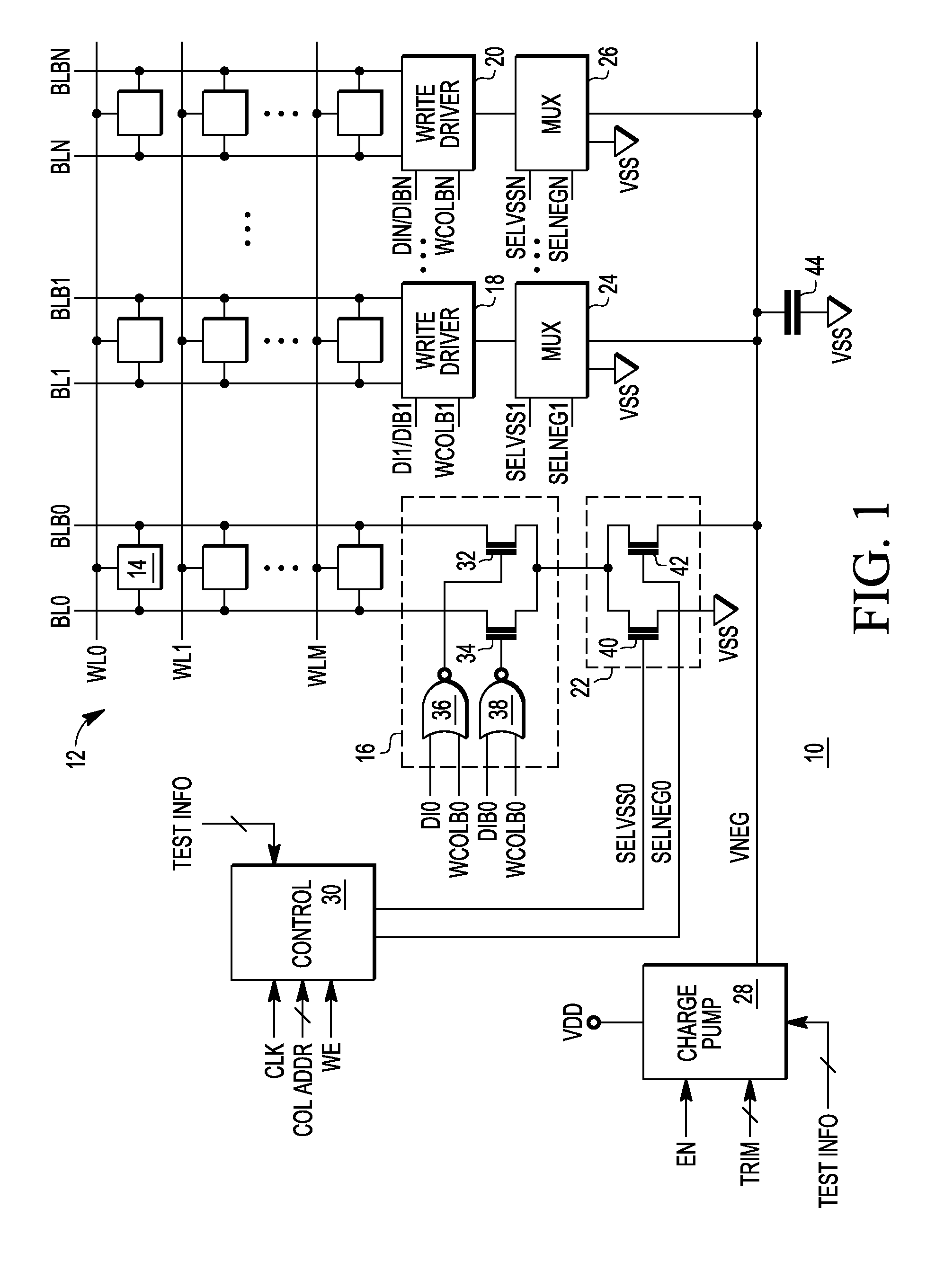
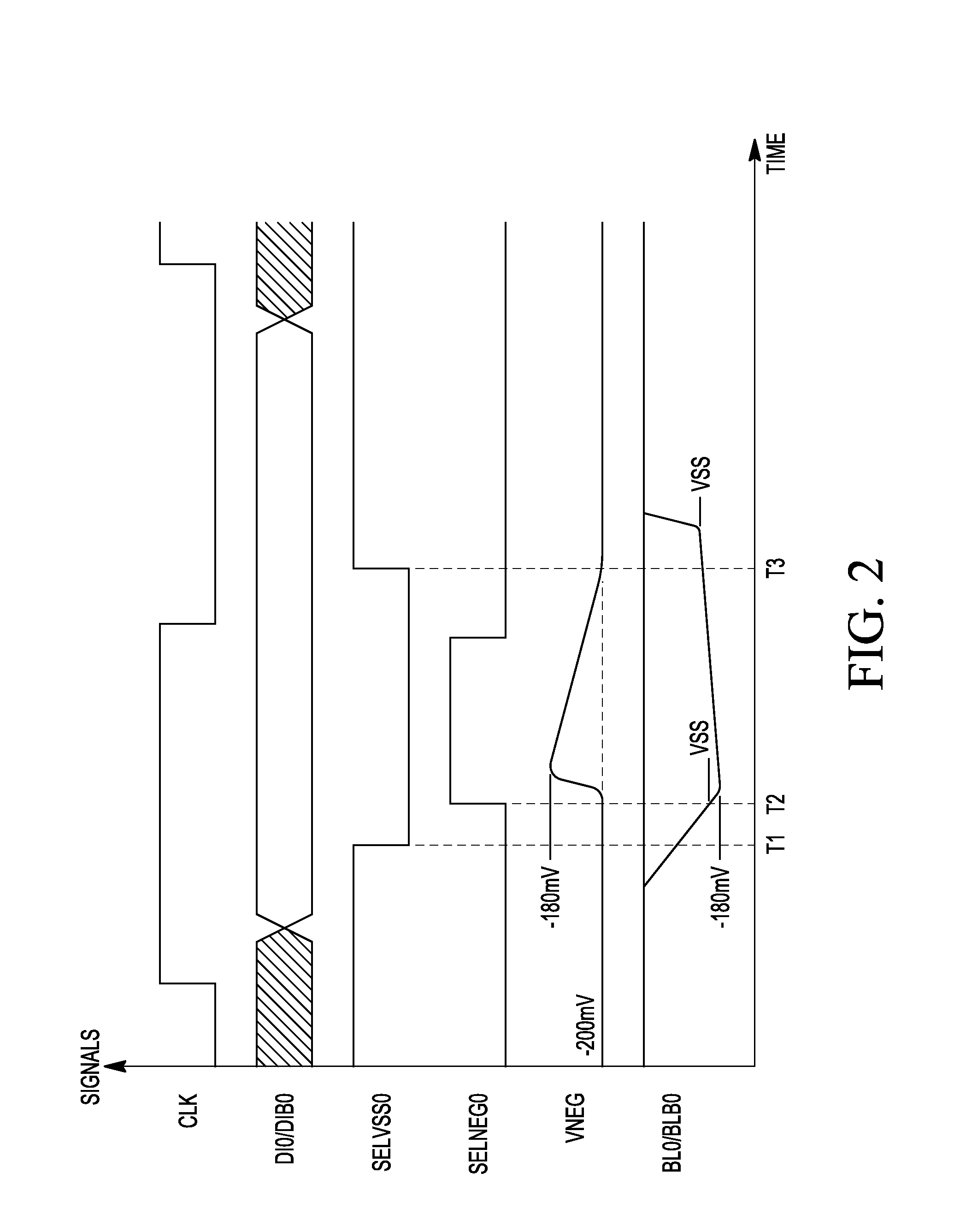
[0011]Generally, there is provided, an integrated circuit memory having a circuit to boost a bit line voltage to below ground level during a write operation. In one embodiment, the circuit includes a charge pump, a multiplexing circuit, and a capacitor. The charge pump generates a negative voltage and continually charges or maintains a predetermined voltage level on the capacitor. During the write operation, the multiplexer receives non-overlapping control signals to cause the bit line to be first pulled to ground, or some other predetermined voltage level, and then to a negative voltage, for example, 200 millivolts (mV). The capacitor is coupled to store negative charge to assist in boosting the bit line voltage below ground. In one embodiment, the memory is a static random access memory (SRAM). Also, in one embodiment, the memory array is first tested for memory cells that are relatively more difficult to write at a predetermined power supply voltage. The locations of those cells ...
PUM
 Abstract
Description
Claims
Application Information