Vacuum thin film forming apparatus

a thin film forming and vacuum technology, applied in vacuum evaporation coatings, electrolysis components, coatings, etc., can solve the problems of inability to keep the plasma state constant, process instability, and difficulty in ensuring process reproducibility, and achieve excellent process reproducibility and high quality

Inactive Publication Date: 2010-08-12
CANON ANELVA CORP
View PDF9 Cites 17 Cited by
  • Summary
  • Abstract
  • Description
  • Claims
  • Application Information

AI Technical Summary

Benefits of technology

[0010]According to the vacuum thin film forming apparatus of the present invention that controls the magnitude of the self-bias applied to the substrate with the variable impedance mechanism, it is possible to automatically adjust the self-bias on the substrate to a constant value at all times and to form a thin film of high quality with excellent process reproducibility.

Problems solved by technology

In the conventional high-frequency sputtering method, it is difficult to ensure process reproducibility when forming an insulating film.
As the insulating film is deposited on the shield and substrate holder, the potential changes with time, and therefore, it is not possible to keep constant the state of plasma and the magnitude of the self-bias on the substrate.
In the case also where the substrate is electrically conductive, the magnitude of self-bias on the substrate changes with time as the insulting film is deposited on the substrate, resulting in instability of process.

Method used


Image

  • Vacuum thin film forming apparatus
  • Vacuum thin film forming apparatus
  • Vacuum thin film forming apparatus

Examples


Embodiment Construction

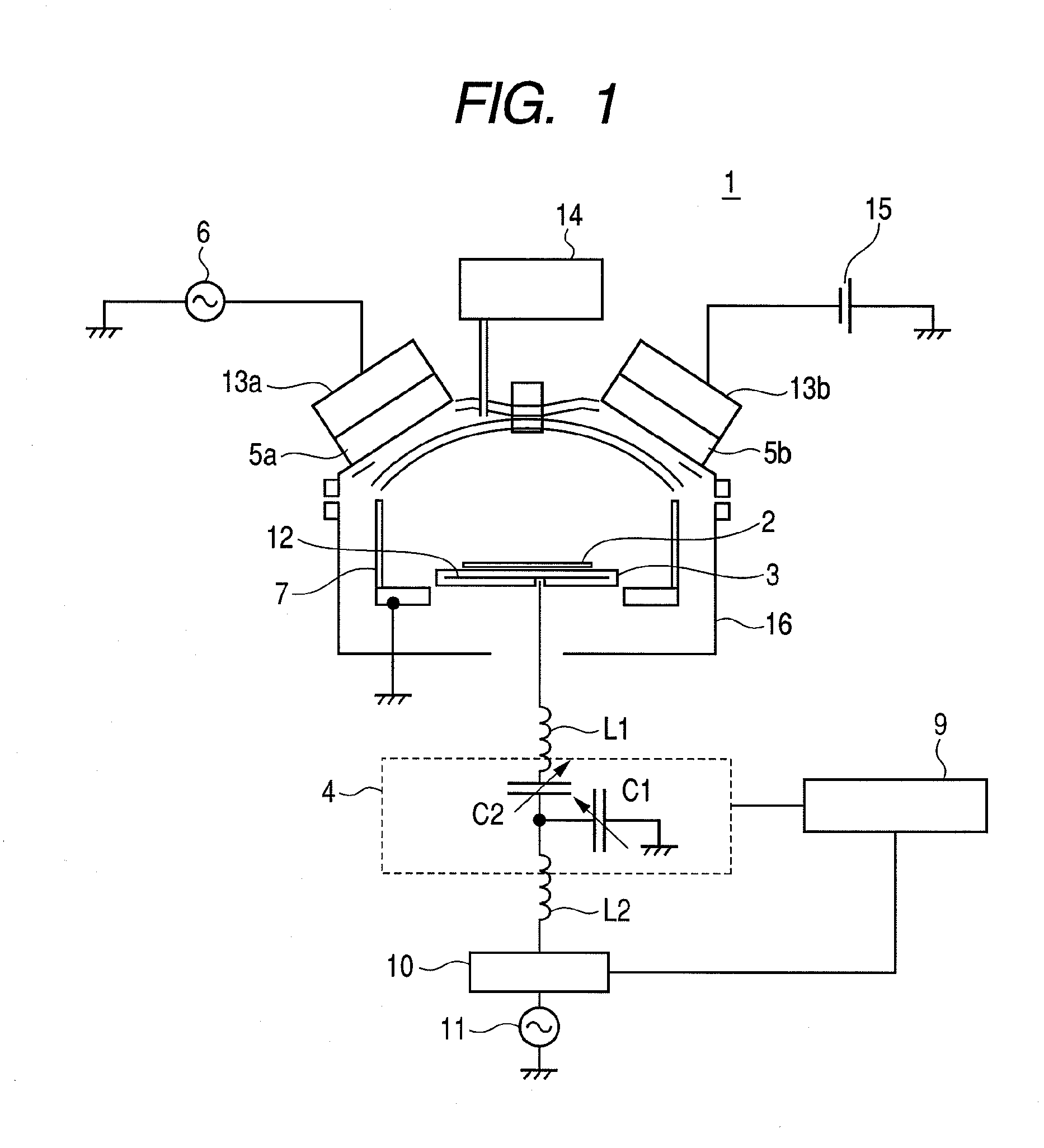
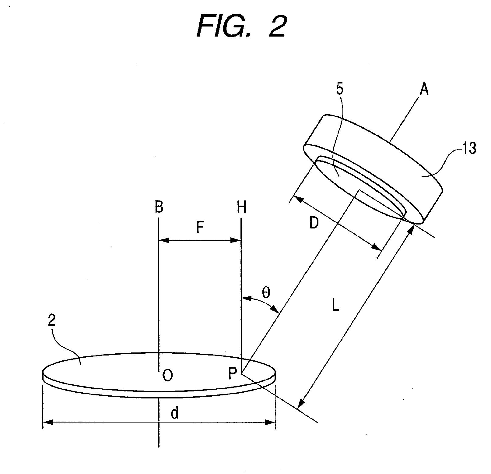
[0024]FIG. 1 is a schematic diagram of a high-frequency sputtering device 1 that exhibits the characteristics of the present invention. The configuration of the high-frequency sputtering device 1 to which the present invention can be applied will be described with reference to FIG. 1. The sputtering device 1 comprises sputtering cathodes 13a and 13b and each of the cathodes 13a and 13b includes a target mounting base. On the target mounting bases of the cathodes 13a and 13b, targets 5a and 5b are mounted, respectively. In the present embodiment, the target 5a is an insulator MgO target and the target 5b is a metal Ta target, however, it is possible for a user to appropriately change the targets by selection. The cathode 13a is connected to a high-frequency power supply 6 and the cathode 13b is connected to a DC power supply 15. The sputtering device 1 further includes a substrate holder 3 provided with a substrate mounting base for mounting a substrate 2 to be subjected to sputterin...


PUM

PropertyMeasurementUnit
distanceaaaaaaaaaa
distanceaaaaaaaaaa
pressureaaaaaaaaaa

Abstract

In order to automatically adjust a self-bias on a substrate to a constant value at all times and to form a high-quality insulating film with excellent process reproducibility, a vacuum thin film forming apparatus according to the present invention includes: a high-frequency sputtering device having a chamber, an evacuation means for evacuating the inside of the chamber, a gas introduction means for supplying gas into the chamber, a substrate holder provided within the chamber, and an electrode provided within the substrate holder; and at least one vacuum treatment chamber that can be selected from a group including a physical vapor deposition (PVD) chamber, a chemical vapor deposition (CVD) chamber, a physical etching chamber, a chemical etching chamber, a substrate heating chamber, a substrate cooling chamber, an oxidation treatment chamber, a reduction treatment chamber, and an ashing chamber, wherein the high-frequency sputtering device further includes a variable impedance mechanism electrically connected to the electrode for adjusting the potential of the substrate on the substrate holder.

Description

CROSS-REFERENCES TO RELATED APPLICATIONS[0001]This application is a continuation application of International Application No. PCT / JP2007 / 069461, filed on Oct. 4, 2007, the entire contents of which are incorporated by reference herein.BACKGROUND OF THE INVENTION[0002]1. Field of the Invention[0003]The present invention relates to a magnetic reproduction head of a magnetic disc drive device, a storage element of a magnetic random access memory, and a magnetic sensor.[0004]2. Related Background Art[0005]A tunnel magnetoresistive thin film using an insulating film MgO as a tunnel barrier layer exhibits a very large magnetoresistive (change) ratio of 200% or more at ambient temperature, and therefore, its application to a reproduction magnetic head and to a storage element of MRAM is expected. There is a demand to reduce the element size for a higher resolution of a magnetic head and a higher integration of MRAM, and it is indispensable to reduce the junction resistance in order to ensur...

Claims


Application Information

Patent Timeline
Patent Type & Authority Applications(United States)
IPC IPC(8): C23C14/34
CPCC23C14/081C23C14/225C23C14/345H01L43/12H01J37/32174H01J37/32706H01J37/34H01J37/32091H10N50/01
Inventor NAGAMINE, YOSHINORINAKAMURA, KANTOTSUNEKAWA, KOJI
Owner CANON ANELVA CORP
Why Eureka
Try Eureka