Check patentability & draft patents in minutes with Patsnap Eureka AI!

High speed detection of shunt defects in photovoltaic and optoelectronic devices

a photovoltaic and optoelectronic technology, applied in photovoltaic monitoring, instruments, air-break switches, etc., can solve the problems of a relatively minor overall degradation of the performance of a properly characterized device, a relatively poor efficiency of end-of-line test cell type, and a regular performance degradation of the devi

Active Publication Date: 2010-08-12
TAU SCI CORP
View PDF6 Cites 52 Cited by
  • Summary
  • Abstract
  • Description
  • Claims
  • Application Information

AI Technical Summary

Benefits of technology

[0028]In another aspect of the invention, determined temperature variations of the DUT are addressed and uniquely analyzed on a pixel-by-pixel basis to provide increased sensitivity at critical locations in the DUT.

Problems solved by technology

Photovoltaic devices regularly exhibit performance degradation due to the presence of current shunts.
These shunts may be induced at various points in the process, such as problems with initial crystalline quality, contact over-firing, surface conduction at crack boundaries, trace metal deposition at the wafer edge, etc.
The resultant defect population usually causes a relatively minor overall degradation of performance of a device that is properly characterized and accounted for during the final test and sort.
This type of cell may exhibit relatively poor efficiency at end of line test due to the network of shunts, but it will not suffer from further degradation due to the shade-induced field degradation mechanism.
Conversely, a cell with similar performance and J-V characteristics as the cell described above may be damaged if the shunts are concentrated in a localized area, or if the shunt defects are large.
In this case, the entire 5 A of reverse bias current flows through a smaller area of silicon, and the higher current density (expressed in Amps / cm2) may cause a local temperature rise that damages the cell within seconds.
The localized heating may also compromise the module lamination layer, allowing moisture to enter the cell and cause freeze / thaw damage or accelerated corrosion.
This damage often results in permanent degradation of cell properties: the cell no longer performs per the original J-V test results, and because the cell is series-connected in the module, the module efficiency is proportionally reduced.
A similar effect occurs in thin-film cells which are monolithically grown and scribed into series-connected cells: partial shading may reverse bias one cell and cause overheating in regions where severe shunts exist.
Thin-film cells often have even poorer thermal conduction characteristics than traditional bulk photovoltaic materials, and so may be more susceptible to this type of field degradation mechanism than the first generation of cells.

Method used


Image

  • High speed detection of shunt defects in photovoltaic and optoelectronic devices
  • High speed detection of shunt defects in photovoltaic and optoelectronic devices
  • High speed detection of shunt defects in photovoltaic and optoelectronic devices

Examples


example # 1

Example #1

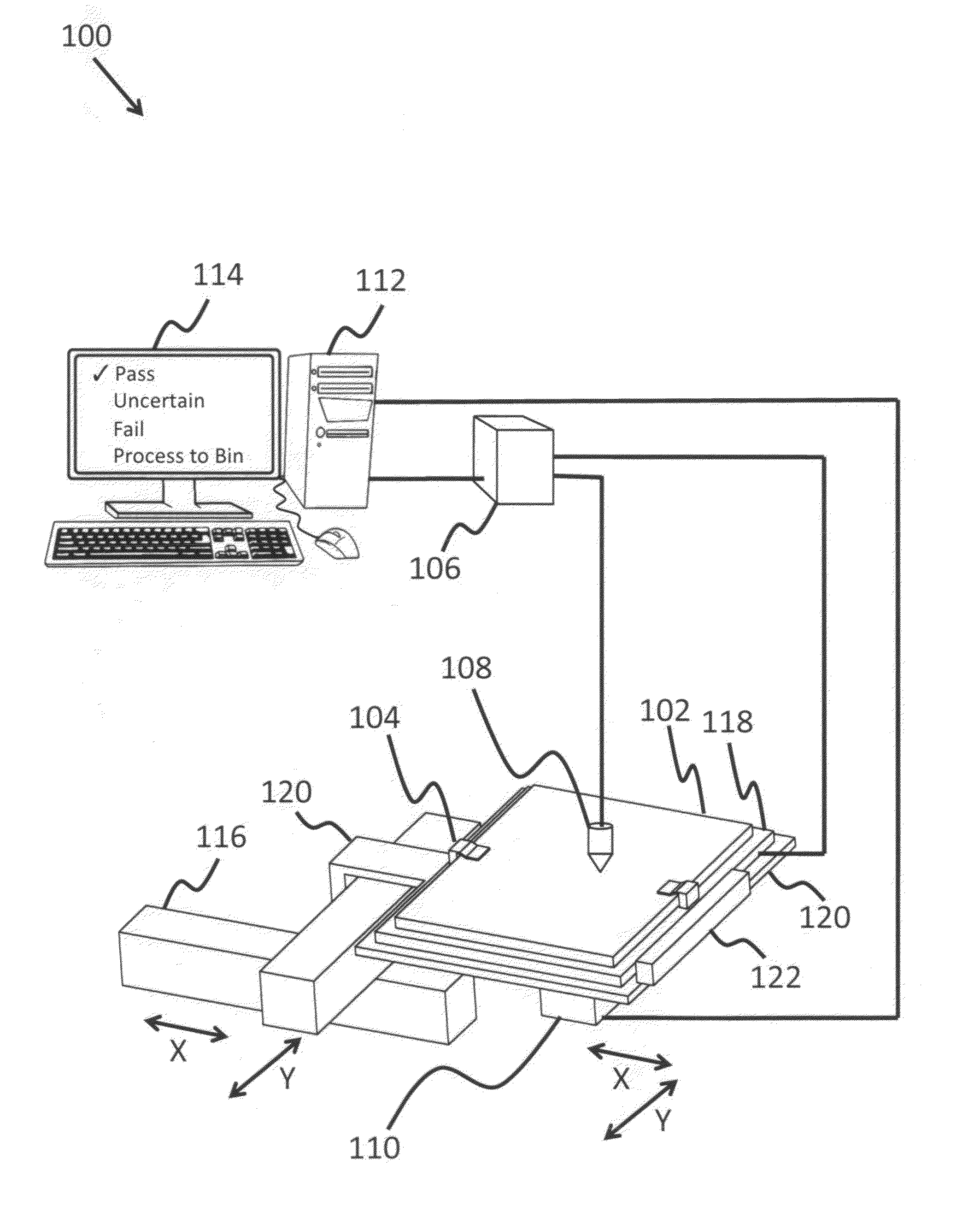
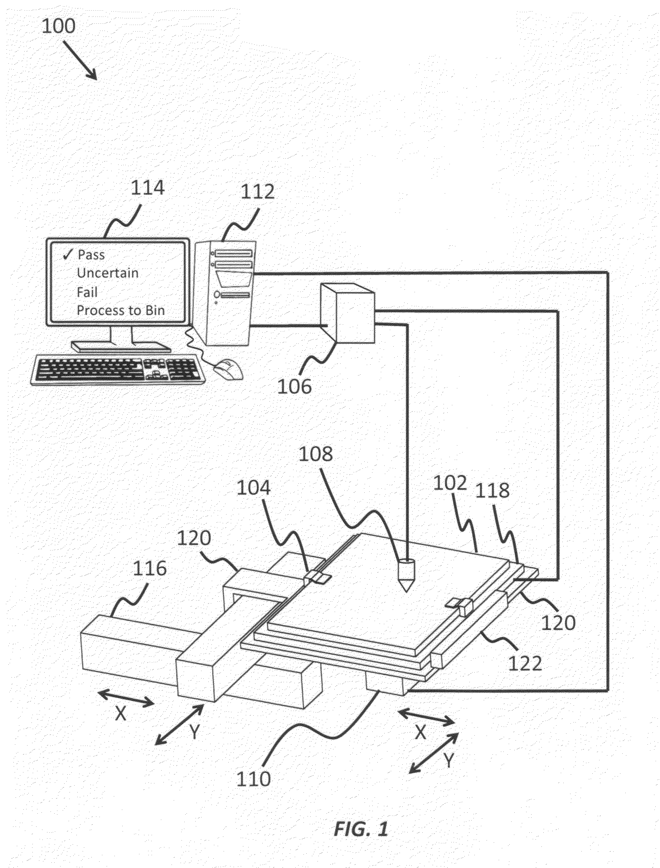
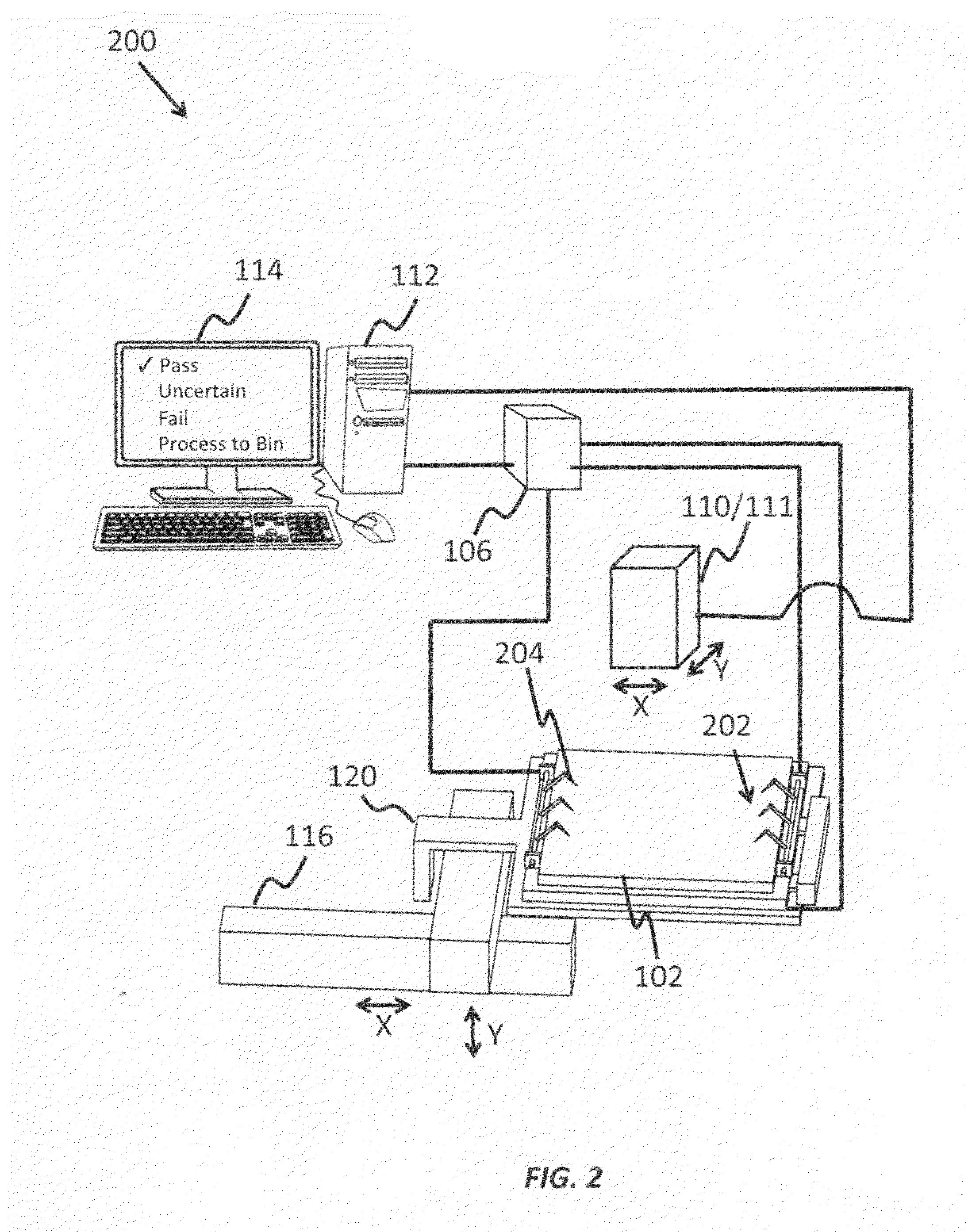
[0075]A step function current of −6 A is applied at time T=0 seconds, and surface temperature images are recorded for a total of 1.5 seconds at intervals of 0.15 seconds. The set of surface temperature images is analyzed to determine the heating rate and / or extrapolate the maximum temperature at each pixel. The set of results from all pixels may then be processed (averaged, spatially filtered to exclude edge effects, spatially analyzed to determine the number and / or proximity of shunts, spatially analyzed to determine the rate of change (in degrees / unit length) as a function of position, binned via histogram to analyze only a portion of the pixels, etc.) to generate the final results such as ‘Pass’, ‘Fail’, ‘Inconclusive’, or a mathematical indicator derived from one or more of the measured parameters that indicates the overheating potential for the cell.

example # 2

Example #2

[0076]A pulsed square-wave voltage waveform is applied to the DUT, with peak voltage=−10V, minimum voltage=0V, and frequency=4.5 Hz. The surface temperature image is measured at a frequency of 9 Hz, and the resultant data is analyzed to determine the heating rate and / or extrapolate the maximum temperature at each pixel. The set of results may then be processed as described in Example #1.

example # 3

Example #3

[0077]A step function current of −4 A is applied at T=0 seconds, and the surface temperature is recorded for a user or algorithm defined time (e.g., 60 seconds) at intervals of 0.15 seconds. The set of surface temperature images is analyzed to find the maximum temperature over the measurement period, as well as the maximum heating rate observed during the measurement. The set of results may then be processed as described in Example #1.

[0078]According to one aspect of the invention, the current-voltage (I-V) or current density-voltage (J-V) characteristics of the cell may also be measured and used as a component of the severity calculation. For instance, cells with large reverse bias current leakage may have a higher potential for overheating than cells with low reverse bias leakage. The following example provides illustration for this aspect with limiting the scope of the invention.


PUM


Abstract

The current invention provides a shunt defect detection device that includes a device under test (DUT) that is fixedly held by a thermally isolating mount, a power source disposed to provide a directional bias condition to the DUT, a probe disposed to provide a localized power to the DUT from the power source, an emission detector disposed to measure a temporal emission from the DUT when in the directional bias condition, where the measured temporal emission is output as temporal data from the emission detector to a suitably programmed computer that uses the temporal data to determine a heating rate of the DUT and is disposed to estimate an overheat risk level of the DUT, where an output from the computer designates the DUT a pass status, an uncertain status, a fail status or a process to bin status according to the overheat risk level.

Description

CROSS-REFERENCE TO RELATED APPLICATIONS[0001]This application is cross-referenced to and claims the benefit from U.S. Provisional Application 61 / 150,737 filed Feb. 7, 2009, which is hereby incorporated by reference.FIELD OF THE INVENTION[0002]The invention relates to detecting defects in optoelectronics. In particular, the invention relates to a method of high-speed imaging to detect critical shunt defects in photovoltaic cells and optoelectronics in manufacturing facilities.BACKGROUND[0003]Photovoltaic devices regularly exhibit performance degradation due to the presence of current shunts. These shunts may be induced at various points in the process, such as problems with initial crystalline quality, contact over-firing, surface conduction at crack boundaries, trace metal deposition at the wafer edge, etc. The resultant defect population usually causes a relatively minor overall degradation of performance of a device that is properly characterized and accounted for during the final...

Claims


Application Information

Patent Timeline
IPC IPC(8): G01R31/04
CPCG01R31/2656H02S50/10G01N21/66Y02E10/50
Inventor VASILYEV, LEONID A.SCHMIDT, JOHN M.HUDSON, JAMES E.HORNER, GREGORY S.
Owner TAU SCI CORP
Features
  • R&D
  • Intellectual Property
  • Life Sciences
  • Materials
  • Tech Scout
  • Unparalleled Data Quality
  • Higher Quality Content
  • 60% Fewer Hallucinations
Learn More