Charged particle beam writing method and charged particle beam writing apparatus

a writing method and charge technology, applied in the field of charged particle beam writing method and charged particle beam writing apparatus, can solve the problems of beam impingement, reducing throughput, and generating reflection electrons

Active Publication Date: 2010-08-19
NUFLARE TECH INC
View PDF6 Cites 9 Cited by
  • Summary
  • Abstract
  • Description
  • Claims
  • Application Information

AI Technical Summary

Benefits of technology

[0014]According to one aspect of the present invention, in a method of writing with a charged particle beam, a predetermined region on which writing is effected by the charged particle beam is divided into smaller regions each consisting of one or the same number of frames, and the areal density of a pattern to be written on each smaller region is determined. The amount of change in pattern areal density between each two adjacent smaller regions is determined, and the smaller regions in the predetermined region are grouped into region groups depending on whether nor not the amount of change is greater than a predetermined value. For each region group, a time profile for compensating for the drift of the charged particle beam is determined. A pattern on the predetermined region is written while compensating for the drift of the charged particle beam for each region group in accordance with the time profile.
[0015]According to another aspect of the present invention, in a charged particle beam writing apparatus which divides a predetermined region on which writing is effected by a charged particle beam into a plurality of region groups and writes a pattern on the predetermined region while compensating for the drift of the charged particle beam in accordance with a time profile for compensating for the drift of the charged particle beam, the time profile being determined for each region group, the charged particle beam writing apparatus comprises grouping means for dividing the predetermined region into smaller regions each consisting of one or the same number of frames, obtaining data indicative of the areal density of a pattern to be written on each smaller region, determining the amount of change in pattern areal density between each two adjacent smaller regions, and grouping the smaller regions into region groups depending on whether or not the amount of change is greater than a predetermined value.

Problems solved by technology

Incidentally, irradiating the mask with the electron beam results in generation of reflection electrons.
This changes the path of the electron beam that has been deflected toward the mask, resulting in displacement of the beam impinging position from the desired target position on the mask, which is referred to as “beam drift.” Although other problems can cause beam drift, in any case it is necessary to make corrections to cause the beam to impinge at the desired location by detecting the reference mark position on the stage in the middle of the writing operation and determining the amount of beam drift.
In this case, however, a reduction in the throughput results.
However, this means that the traveling speed of the stage is not constant, making it difficult to estimate the time of completion of the writing operation.
However, the estimation is difficult if the areal density of the pattern varies from one writing region to another.
However, the estimation is difficult if the areal density of the pattern varies.
The above publication only discloses a method of determining the time intervals at which to make a drift compensation for each writing region in the pattern writing field and therefore fails to provide a technique for improving the writing accuracy of the electron beam writing apparatus.

Method used


Image

  • Charged particle beam writing method and charged particle beam writing apparatus
  • Charged particle beam writing method and charged particle beam writing apparatus
  • Charged particle beam writing method and charged particle beam writing apparatus

Examples


Embodiment Construction

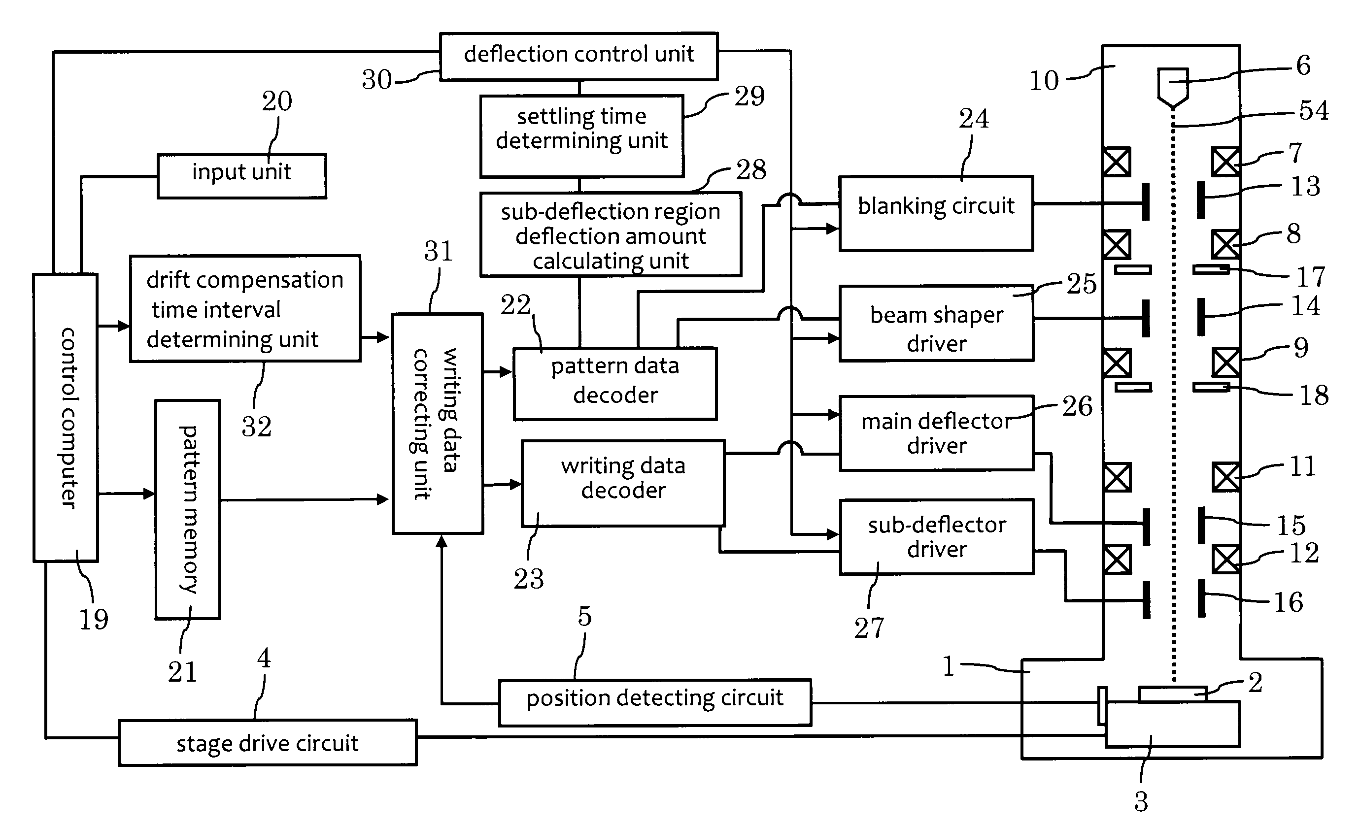
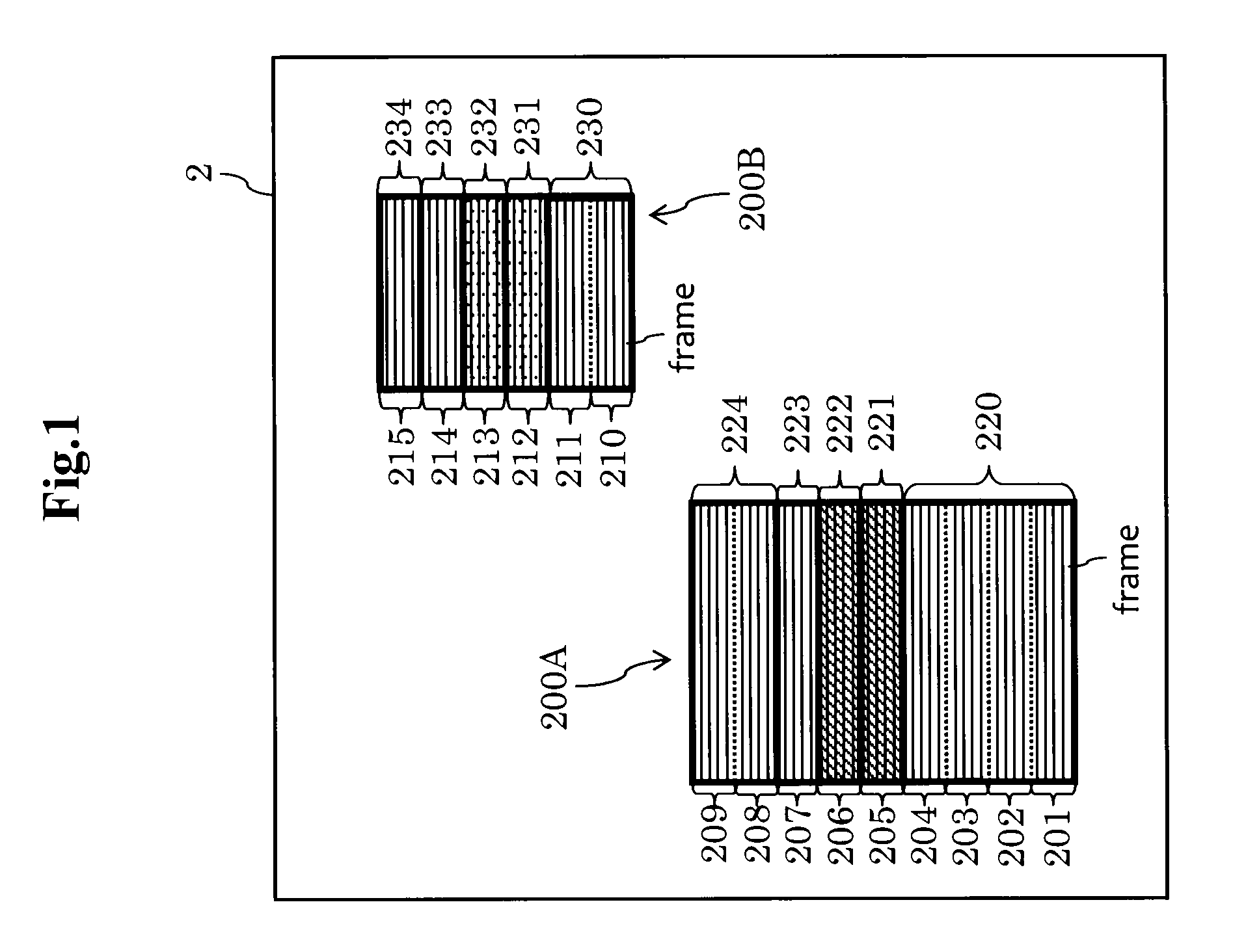
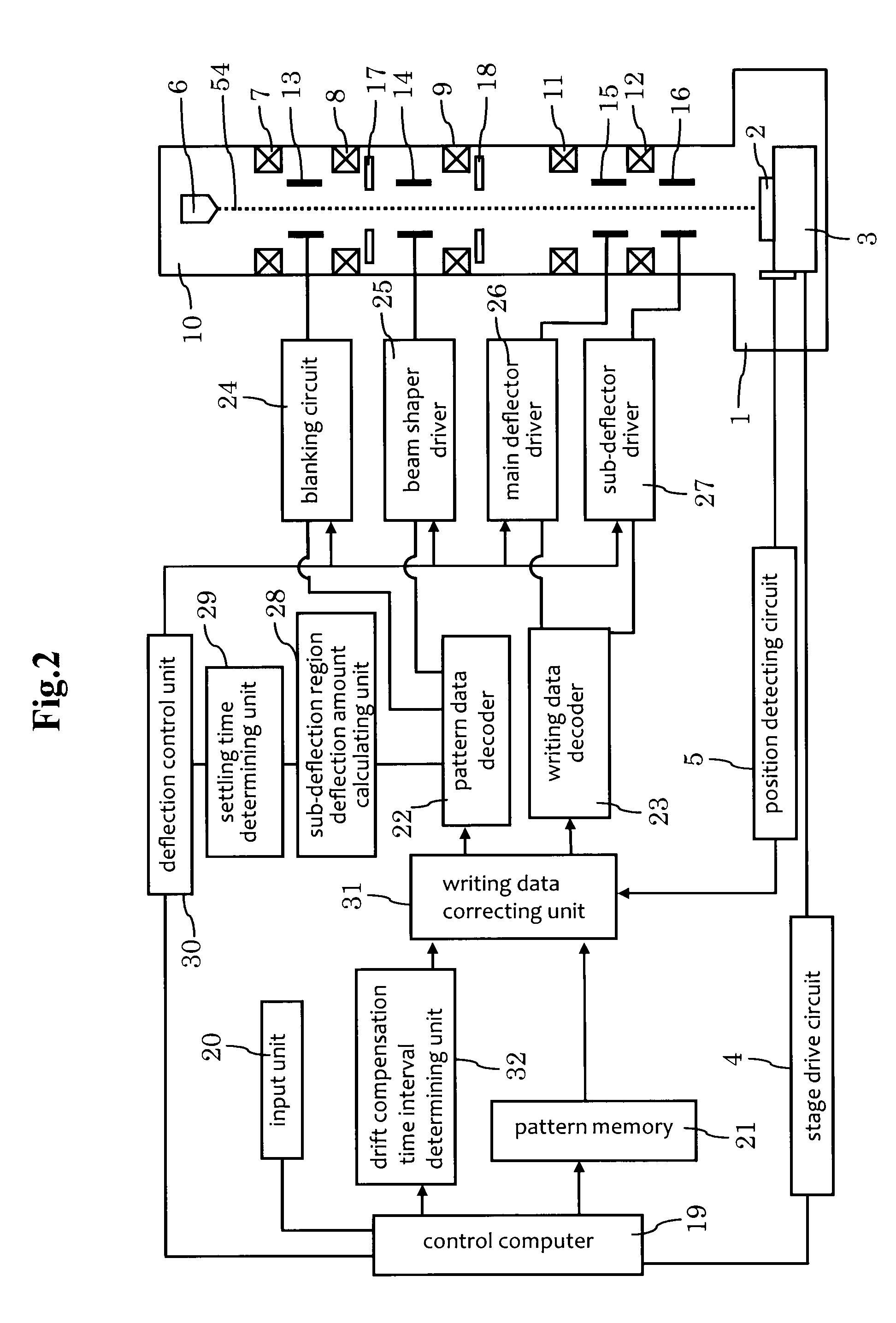
[0020]An electron beam writing method of an embodiment of the present invention begins by dividing a predetermined region on which writing is effected by an electron beam into smaller regions each consisting of one or the same number of frames. The method then determines the areal density of a pattern to be written on each smaller region. The next step determines the amount of change in pattern areal density between each two adjacent smaller regions, and groups these smaller regions into region groups depending on whether or not the amount of change in pattern areal density is greater than a predetermined value. The method then determines, for each region group, a time profile for compensating for the drift of the electron beam. It should be noted that in this specification, if the pattern areal density in one region is lower than that in the preceding region, the amount of change in pattern areal density between these regions is defined to be negative. On the other hand, if the pat...


PUM

PropertyMeasurementUnit
areal densityaaaaaaaaaa
widthaaaaaaaaaa
wavelengthaaaaaaaaaa

Abstract

Based on the pattern writing data input to an input unit 20, a control computer 19 divides a predetermined region on which writing is effected by an electron beam 54 into smaller regions each consisting of one or the same number of frames and determines the areal density of a pattern to be written on each smaller region. A drift compensation time interval determining unit 32 then determines the amount of change in pattern areal density between each two adjacent smaller regions, and groups the smaller regions in the predetermined region into region groups depending on whether or not the amount of change is greater than a predetermined value. A time profile for compensating for the drift of the electron beam 54 is then determined for each region group.

Description

BACKGROUND OF THE INVENTION[0001]1. Field of the Invention[0002]The present invention relates to a charged particle beam writing method and a charged particle beam writing apparatus.[0003]2. Background Art[0004]Recently, along with the development of higher levels of integration in semiconductor devices, the dimensions of the individual component devices have decreased and so has the width of wires and gates making up these components.[0005]Photolithographic techniques which help achieve such miniaturization include the following sequential processes: applying a resist material to the surface of the substrate to be processed to form a resist film; irradiating the substrate with light or an electron beam to expose a predetermined resist pattern to form a latent image; heating the substrate as necessary; developing the pattern to form a micropattern; and etching the substrate using this micropattern as a mask.[0006]In photolithography, the minimum width of a wiring pattern, etc. that ...

Claims


Application Information

Patent Timeline
Patent Type & Authority Applications(United States)
IPC IPC(8): G03F7/20G21K5/04
CPCB82Y10/00H01J37/3174B82Y40/00G03F7/2022G03F7/203G03F7/70433G03F7/7045G03F7/7055
Inventor KUROHORI, TAKESHI
Owner NUFLARE TECH INC
Why Eureka
Try Eureka