Method For Producing An Electro-Optical Printed Circuit Board With Optical Waveguide Structures

Active Publication Date: 2010-08-19
VARIO OPTICS
View PDF10 Cites 16 Cited by
  • Summary
  • Abstract
  • Description
  • Claims
  • Application Information

AI Technical Summary

Benefits of technology

[0011]The reference marks can be used in order to produce depressions and/or holes in the printed circuit board by mecha

Problems solved by technology

As a result of the transparency, the optical waveguide structures cannot be detected by means of image recognition systems during the mounting of the components.
A precise alignment of electro-optical components such as LE

Method used


Image

  • Method For Producing An Electro-Optical Printed Circuit Board With Optical Waveguide Structures
  • Method For Producing An Electro-Optical Printed Circuit Board With Optical Waveguide Structures
  • Method For Producing An Electro-Optical Printed Circuit Board With Optical Waveguide Structures

Examples


Embodiment Construction

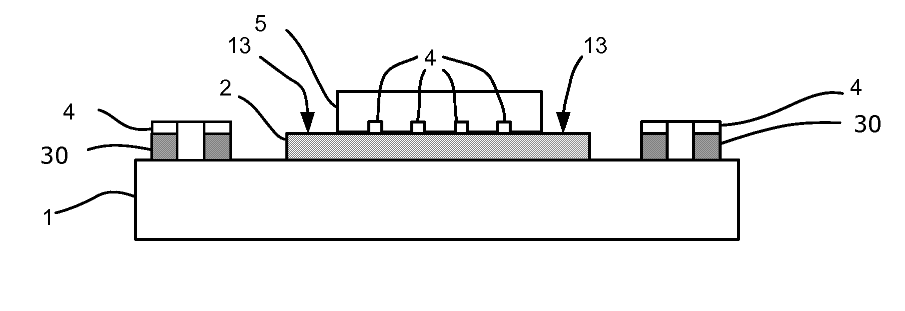
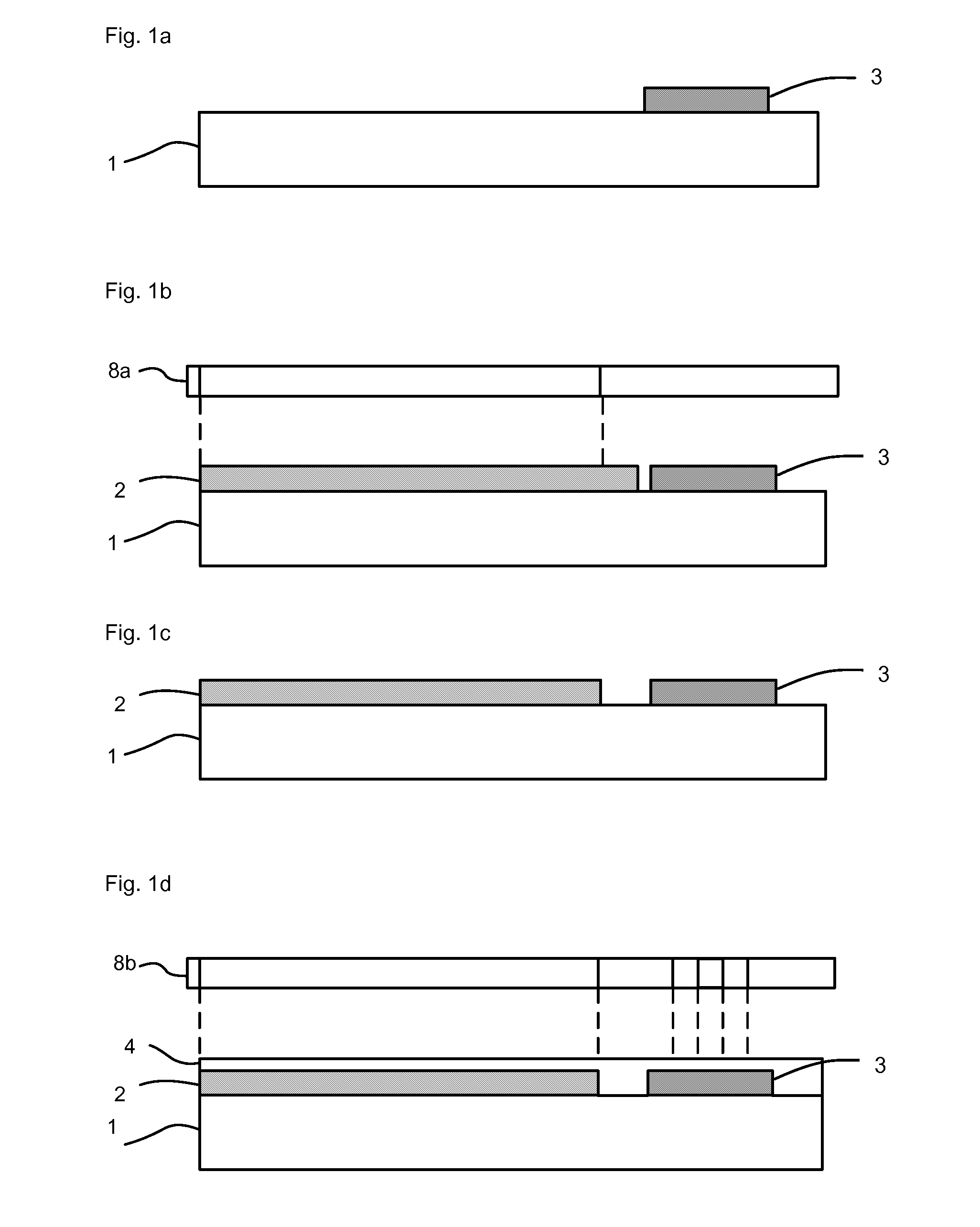
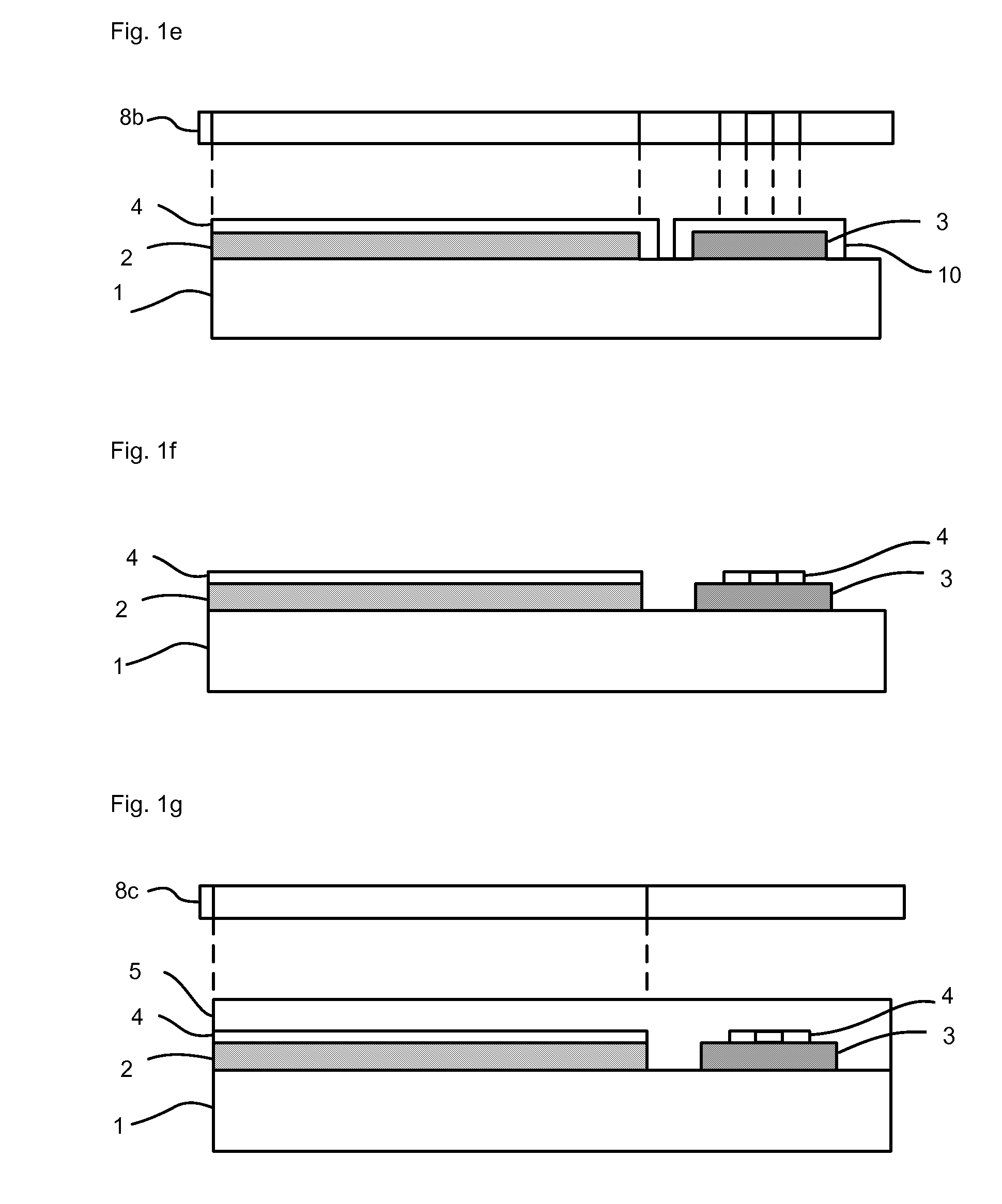
[0032]An electro-optical printed circuit board with optical waveguide structures consists of a substrate 1, on which metallic structures, especially tracks, for the electrical connection of electronic and electro-optical components are arranged on the one hand and optical waveguide structures on the other hand. The substrate 1 consists for example of FR4, polyimide or any other suitable material.

[0033]The method in accordance with the invention for producing an electro-optical printed circuit board with optical waveguide structures comprises the method steps A through F and optionally the method step G, which shall be explained below in detail by reference to FIGS. 1a to 1k: [0034]A) Forming non-transparent areas 3 on the substrate 1.

With this step a non-transparent material is disposed over the substrate 1 and, if necessary, structured such that non-transparent areas 3 are formed on the substrate 1. The state after this step is shown in FIG. 1 a.

[0035]The optical waveguide structur...


PUM


Abstract

An electro-optical printed circuit board contains electrical conductor tracks on the one hand and optical waveguide structures on the other hand. The optical waveguide structures comprise a bottom layer, a core layer and a cladding layer. Visible areas are applied to the printed circuit board, and the core layer is applied later both to the bottom layer as well as the visible areas and structured both on the bottom layer as well as the visible areas. This structure is then transferred to the visible areas, e.g. by etching. Reference marks are thus produced which contain the information on the actual position of the optical waveguide structures.

Description

PRIORITY CLAIM[0001]The present application is related to and claims foreign priority under 35 U.S.C §119 from Swiss Patent Application No. 251 / 09 filed Feb. 17, 2009 and from Swiss Patent Application No. 1508 / 09 filed Sep. 30, 2009, the disclosures of which are herein incorporated by reference.FIELD OF THE INVENTION[0002]The present invention concerns a method for producing an electro-optical printed circuit board with optical waveguide structures.BACKGROUND OF THE INVENTION[0003]The electro-optical printed circuit board technology relates to the production of printed circuit boards which connect electronic, electro-optical and optical components with one another. They contain electrical conductor tracks on the one hand and optical waveguide structures on the other hand.[0004]Optical waveguide structures consist of a plurality of transparent layers, which are usually three layers, made of UV-curing polymer materials with different refractive indexes. As a result of the transparency...

Claims


Application Information

Patent Timeline
IPC IPC(8): G03F7/20
CPCG02B6/136G02B6/42G02B6/4224G02B6/423G02B2006/12173H05K2201/09918H05K1/0274H05K3/0032H05K3/0047H05K3/061H05K2201/09781H05K1/0269C23F1/02
Inventor BETSCHON, FELIXHALTER, MARKUS
Owner VARIO OPTICS
Why Eureka
Try Eureka