Interaction Detecting Portion with Electrode Having the Same Potential, Sensor Chip Using the Same, and Interaction Detector

a technology of interaction detection and electrode, applied in the field of technology, can solve the problems of difficult to exert the desired electrodynamic effect on the entire reaction region, the structure of the reaction region becomes more complicated, and the reaction region in the sensor chip such as the dna chip or the protein chip is generally limited, so as to achieve the effect of simplifying the structure of the detection portion, simplifying the structure of the detector, and less morphologic restrictions

Inactive Publication Date: 2010-08-26
SONY CORP
View PDF1 Cites 3 Cited by
  • Summary
  • Abstract
  • Description
  • Claims
  • Application Information

AI Technical Summary

Benefits of technology

[0024]The present invention adopts the structure that the electrode (that is, the counter electrode) disposed so as to face the reaction region is not provided, but the electrode or the group of electrodes having the same potential is provided. As a result, the applied electric field (electric lines of force) can be made to diverge in all the directions in the vicinity of the electrode. That is to say, since the electric field (electric lines of force) can be made to diverge far and wide toward the entire reaction region, the electrical gradient, or the nonuniform electric field can be formed in the entire reaction region. As a result, the materials dispersed in the reaction region can be efficiently collected up in larger numbers to the electrode side through the electrodynamic migration action.
[0025]Since it is unnecessary to form the counter electrode in the reaction region, the number of morphologic restrictions to the reaction region is less, and thus the structure of the detection portion can be simplified. For example, in the electric field applying means, with respect to the power feeding wiring itself, the grounding portion has to be previously connected to the system side, and the wiring for the detection portion has to be connected to only the electrode in the hybridization region. As a result, the structure of the detector can also be simplified.

Problems solved by technology

Therefore, each of the prior arts described above involves a technical problem that it is difficult to exert the desired electrodynamic effect on the entire reaction region because the electric field (electric lines of force) is generated across the counter electrodes.
In addition, the reaction region in the sensor chip such as the DNA chip or the protein chip is generally limited.
Hence, when the electrode or the group of electrodes showing the counter disposition relationship with the reaction region are provided, there are encountered technical problems: (1) The structure of the reaction region becomes more complicated, (2) the morphologic restriction to the reaction region occurs because of the formation of the counter electrode, (3) the number of processes for manufacturing the chip increases, (4) the distribution of the electric supply line to the electrodes is also complicated, and so forth.

Method used


Image

  • Interaction Detecting Portion with Electrode Having the Same Potential, Sensor Chip Using the Same, and Interaction Detector
  • Interaction Detecting Portion with Electrode Having the Same Potential, Sensor Chip Using the Same, and Interaction Detector
  • Interaction Detecting Portion with Electrode Having the Same Potential, Sensor Chip Using the Same, and Interaction Detector

Examples


Embodiment Construction

[0041]Hereinafter, preferred embodiments for carrying out the present invention will be described with reference to the accompanying drawings. It is noted that each of embodiments shown in the accompanying drawings merely shows an example of a typical embodiment of a product or a method relating to the present invention, and thus the scope of the present invention is not intended to be construed in a limiting sense.

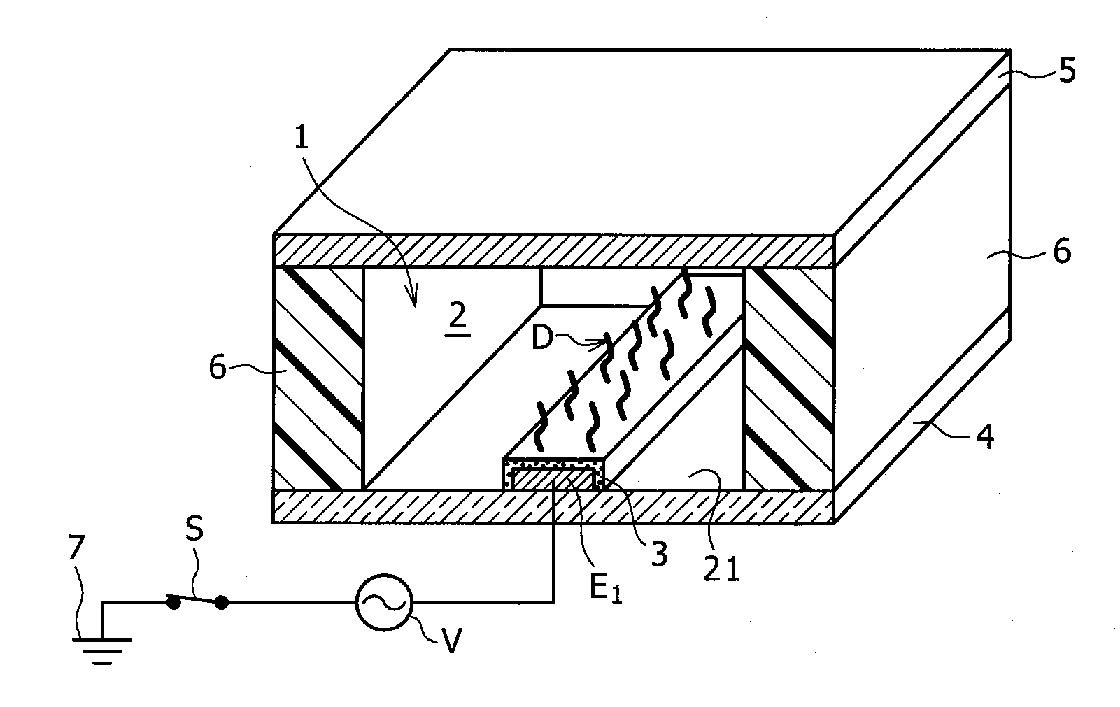
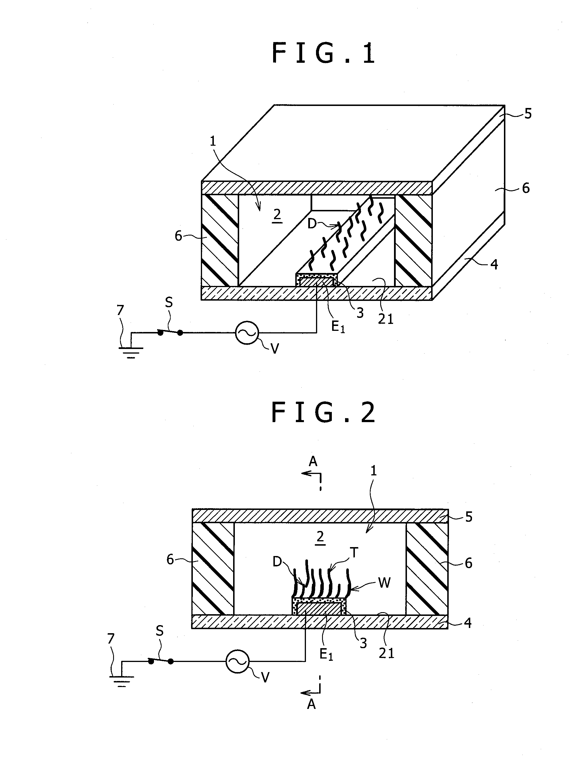
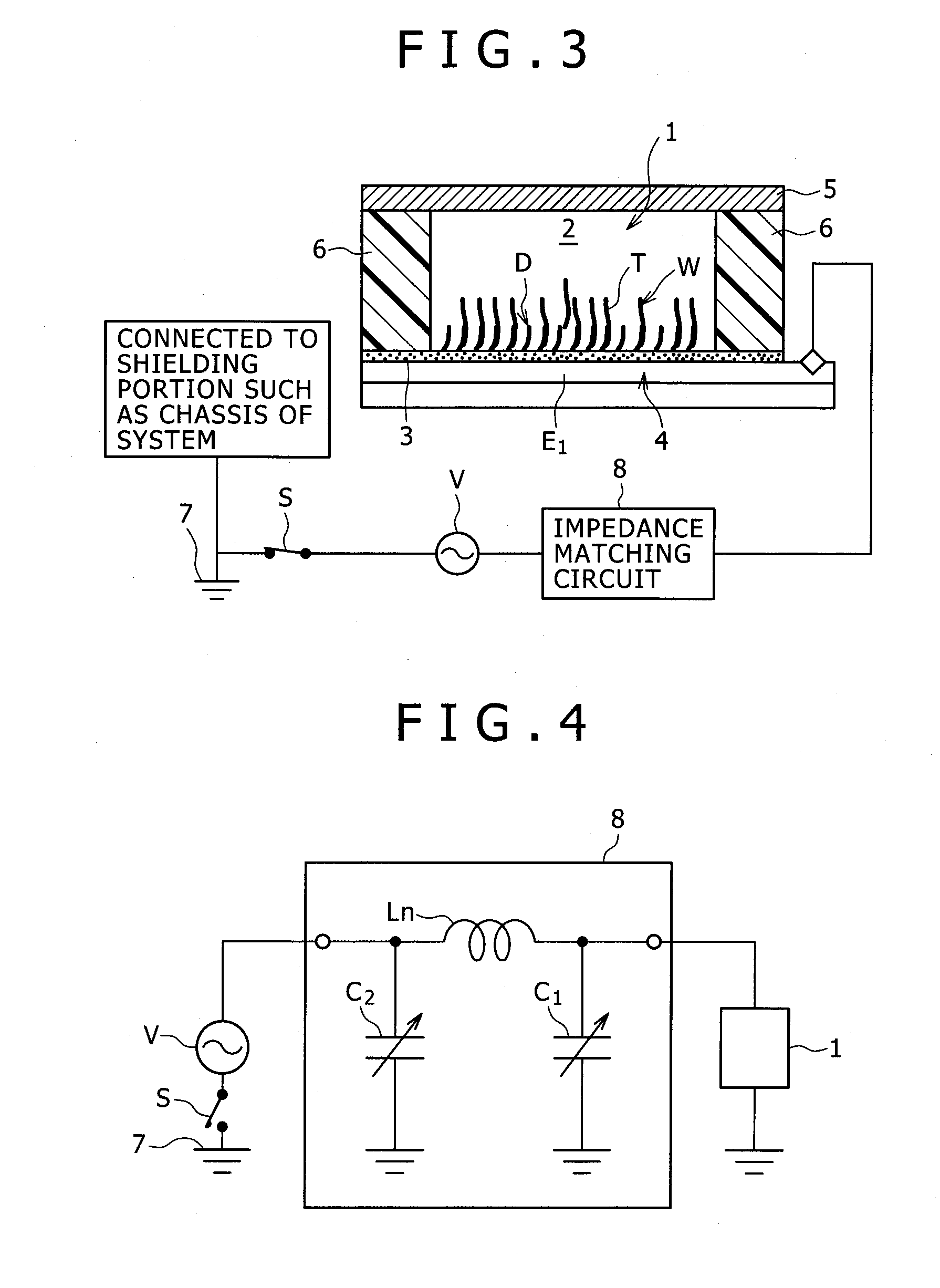
[0042]FIG. 1 is a main portion cubic perspective view explaining a basic constitution of a first embodiment as an interaction detecting portion (hereinafter referred to as “a detection portion”) according to the present invention, FIG. 2 is a transverse cross sectional view of the detection portion, and FIG. 3 is a cross sectional view taken on line A-A of FIG. 2.

[0043]Firstly, FIGS. 1 to 3 show the preferred first embodiment of the detection portion 1 according to the present invention. As shown in these figures, a reaction region 2 having a well shape (inverse recess sh...


PUM

PropertyMeasurementUnit
diameteraaaaaaaaaa
diameteraaaaaaaaaa
diameteraaaaaaaaaa

Abstract

There are provided an interaction detecting portion including an interaction region in the whole of which an electrodynamic effect is obtained, and which has a simpler structure, and the like. There is provided an interaction detecting portion 1 including at least: a reaction region 2 which provides a field for an interaction between materials, and an electrode E1 (or a group of electrodes), having the same potential, which is provided so as to face the reaction region 2. In addition, there are provided a sensor chip, such as a DNA chip or a protein chip, including the interaction detecting portion 1, and an interaction detector using the detection portion 1.

Description

TECHNICAL FIELD[0001]The present invention relates to a technique for detecting an interaction between materials. More specifically, the invention relates to a technique for detecting an interaction between materials by utilizing an electrodynamic action.BACKGROUND ART[0002]In recent years, an integrated substrate for bioassay so-called a DNA chip or a DNA microarray (hereinafter generally referred to as “a DNA chip” in this application) in which predetermined DNAs are finely arranged by utilizing a microarray technique has been utilized for an analysis of mutation of a gene, an analysis of SNPs (single nucleotide polymorphisms), an analysis of a frequency of genomic expression, and the like. Also, the DNA chip begins to be generally used in the fields of a drug discovery, a clinical diagnosis, a pharmacogenomics, a research of evolution, a forensic medicine, and the others.[0003]The feature of this “DNA chip” is that an exhaustive analysis of a hybridization becomes possible becaus...

Claims


Application Information

Patent Timeline
Patent Type & Authority Applications(United States)
IPC IPC(8): G01N27/26G01N27/447
CPCB01L3/5027G01N27/4473G01N33/5438C12Q1/6813C12Q1/6837G01N21/78G01N33/53G01N33/5302
Inventor SEGAWA, YUJIKATSUMOTO, YOICHI
Owner SONY CORP
Why Eureka
Try Eureka