Memory device and operation method of the same

Active Publication Date: 2010-08-26
SONY SEMICON SOLUTIONS CORP
View PDF4 Cites 18 Cited by
  • Summary
  • Abstract
  • Description
  • Claims
  • Application Information

AI Technical Summary

Benefits of technology

[0038]In accordance with the embodiment of the present invention, it is possible to provide a memory device including a circuit capable of executing the inhibit control with a high degree of reliability and at a high speed in accordance with a determination result produced in a direct verify sub-operation.
[0039]In addition, i

Problems solved by technology

In accordance with the method disclosed in Patent Document 1, since the verify sub-operation is carried out after waiting for time to lapse since the application of an update pulse, the method is not suitable

Method used


Image

  • Memory device and operation method of the same
  • Memory device and operation method of the same
  • Memory device and operation method of the same

Examples


Example

1: First Embodiment

[0064]The first embodiment implements a configuration in which a (verify-pass) latch circuit 74 is provided at a location in close proximity to a sense amplifier. FIGS. 10 to 14 are referred to in the explanation of the first embodiment.

Example

2: Second Embodiment

[0065]The second embodiment implements a configuration in which the (verify pass) latch circuit 74 is not created at a location in close proximity to a sense amplifier, but replaced by an external logic circuit which serves as a substitute for the latch. FIGS. 15 to 19 are referred to in the explanation of the second embodiment.

3: First Modified Version

[0066]As shown in a circuit diagram of FIG. 20, a first modified version has a configuration including a sense latch circuit 71A which employs two MOS transistors 22 which each have a MOS gate serving as an input terminal.

4: Second Modified Version

[0067]As shown in diagrams of FIGS. 21 and 22, a second modified version implements typical wiring of SAs (sense amplifiers).

1: First Embodiment

Memory-Cell Configuration

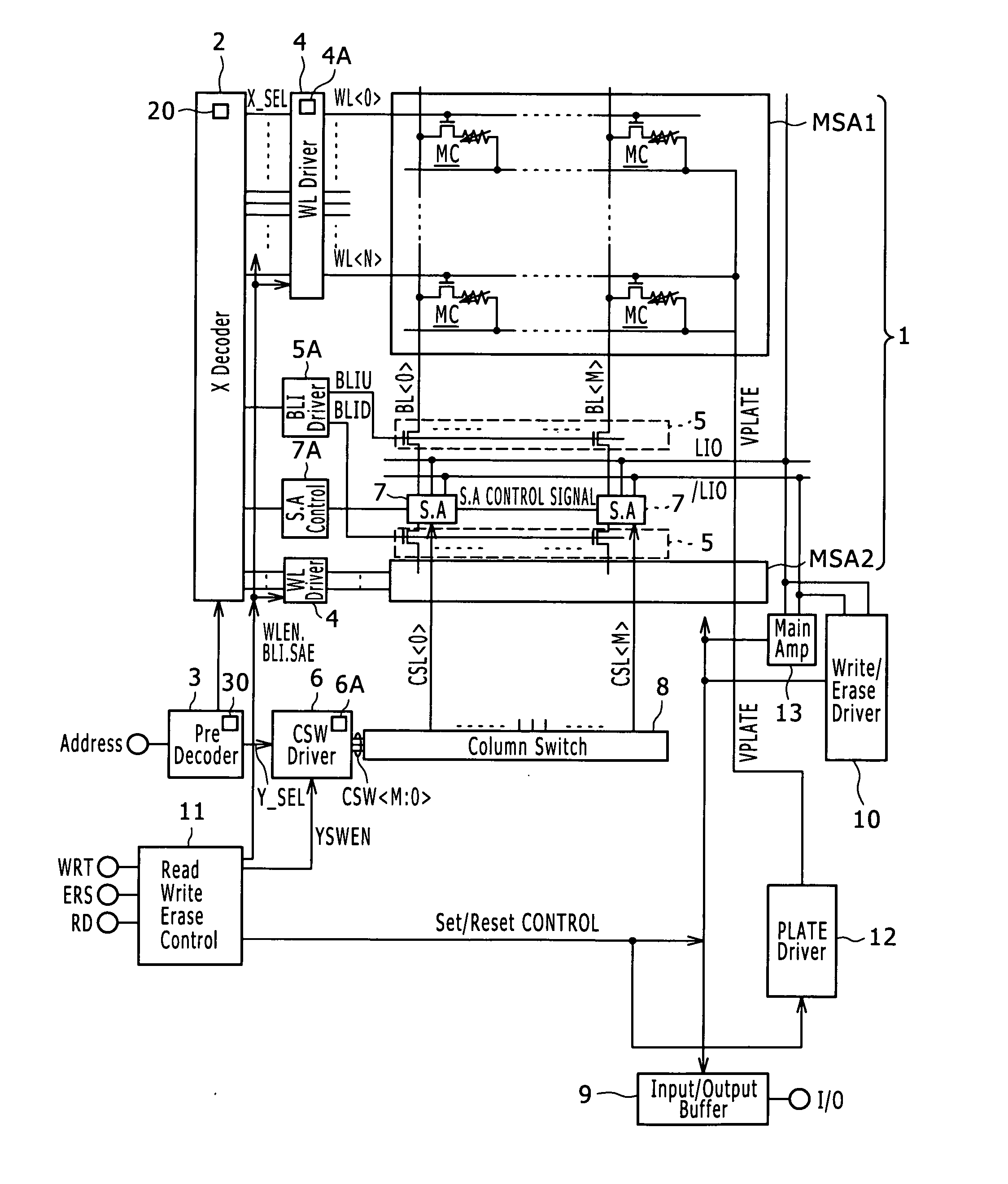
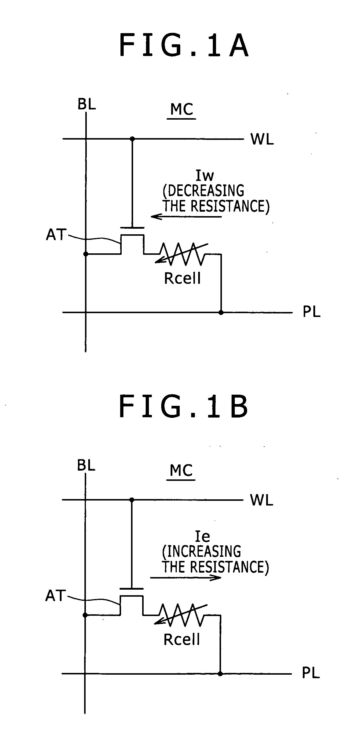
[0068]FIGS. 1A and 1B are a plurality of circuit diagrams each showing an equivalent circuit of a memory cell MC which is common to first and second embodiments as well as modified versions of the embodime...


PUM


Abstract

Disclosed herein is a memory device including: first and second wires; memory cells including a variable-resistance storage element having a data storage state making a transition by a change of a voltage applied and an access transistor connected in series between the first and second wires; driving control sections controlling a direct verify sub-operation by applying a write/erase pulse between the first and second wires in a data write/erase operation respectively for causing a cell current to flow between the first and second wires through the memory cell for a transition of the data storage state; sense amplifiers sensing an electric-potential change occurring on the first wire in accordance with control on the direct verify sub-operation; and inhibit control sections determining whether or not to inhibit a sense node of the sense amplifier from electrically changing at the next sensing time on the basis of an electric potential appearing at the sense node at the present sensing time.

Description

BACKGROUND OF THE INVENTION[0001]1. Field of the Invention[0002]The present invention relates to a memory device employing memory cells each including a variable-resistance storage element which has a resistance changing in accordance with a voltage applied to the variable-resistance storage element and is connected in series to an access transistor, and relates to a method for operating the memory device.[0003]2. Description of the Related Art[0004]There has been already known a memory device employing memory cells each including a variable-resistance storage element which has a resistance changing due to injection of conductive ions into an insulation film of the variable-resistance storage element or due to extraction of such ions from the insulation film. For more information on this memory device, the reader is suggested to refer to a document such as K. Aratani etc., “A Novel Resistance-type memory with High Scalability and Nanosecond Switching,” Technical Digest IEDM 2007, pp...

Claims


Application Information

Patent Timeline
IPC IPC(8): G11C11/00G11C7/00G11C7/10
CPCG11C13/0009G11C13/0026G11C13/004G11C2213/79G11C2213/11G11C2213/34G11C2213/56G11C13/0064
Inventor KITAGAWA, MAKOTOSHIIMOTO, TSUNENORI
Owner SONY SEMICON SOLUTIONS CORP
Why Eureka
Try Eureka