Organic el device

Active Publication Date: 2010-09-02
IDEMITSU KOSAN CO LTD
View PDF12 Cites 60 Cited by
  • Summary
  • Abstract
  • Description
  • Claims
  • Application Information

AI Technical Summary

Benefits of technology

[0019]An object of the invention is to solve the above problems and provide an organic EL device to emit phosphorescence of high efficiency and long lifetime. Specifically, an object of the invention is to provide a phosphorescent organic EL device in which a hole transpo

Problems solved by technology

The concentration of the electron may promote degradation of the materials and reduce lifetime of the device.
As such a material, tris-4,4′,4″-

Method used


Image

  • Organic el device
  • Organic el device
  • Organic el device

Examples


example 1

[0165]A glass substrate (size: 25 mm×75 mm×1.1 mm thick) having an ITO transparent electrode (manufactured by Asahi Glass Co., Ltd) was ultrasonic-cleaned in isopropyl alcohol for five minutes, and then UV / ozone-cleaned for 30 minutes.

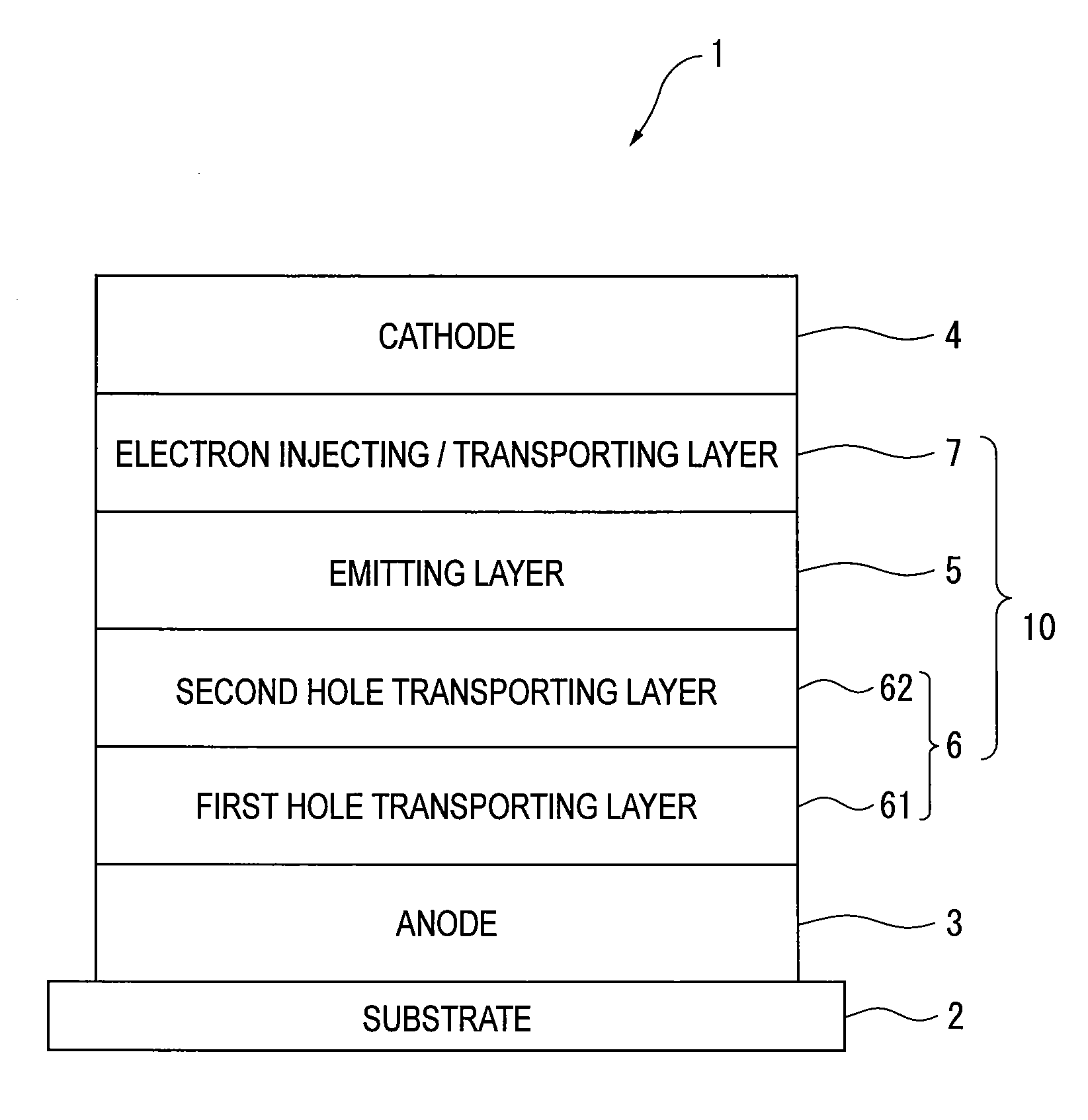
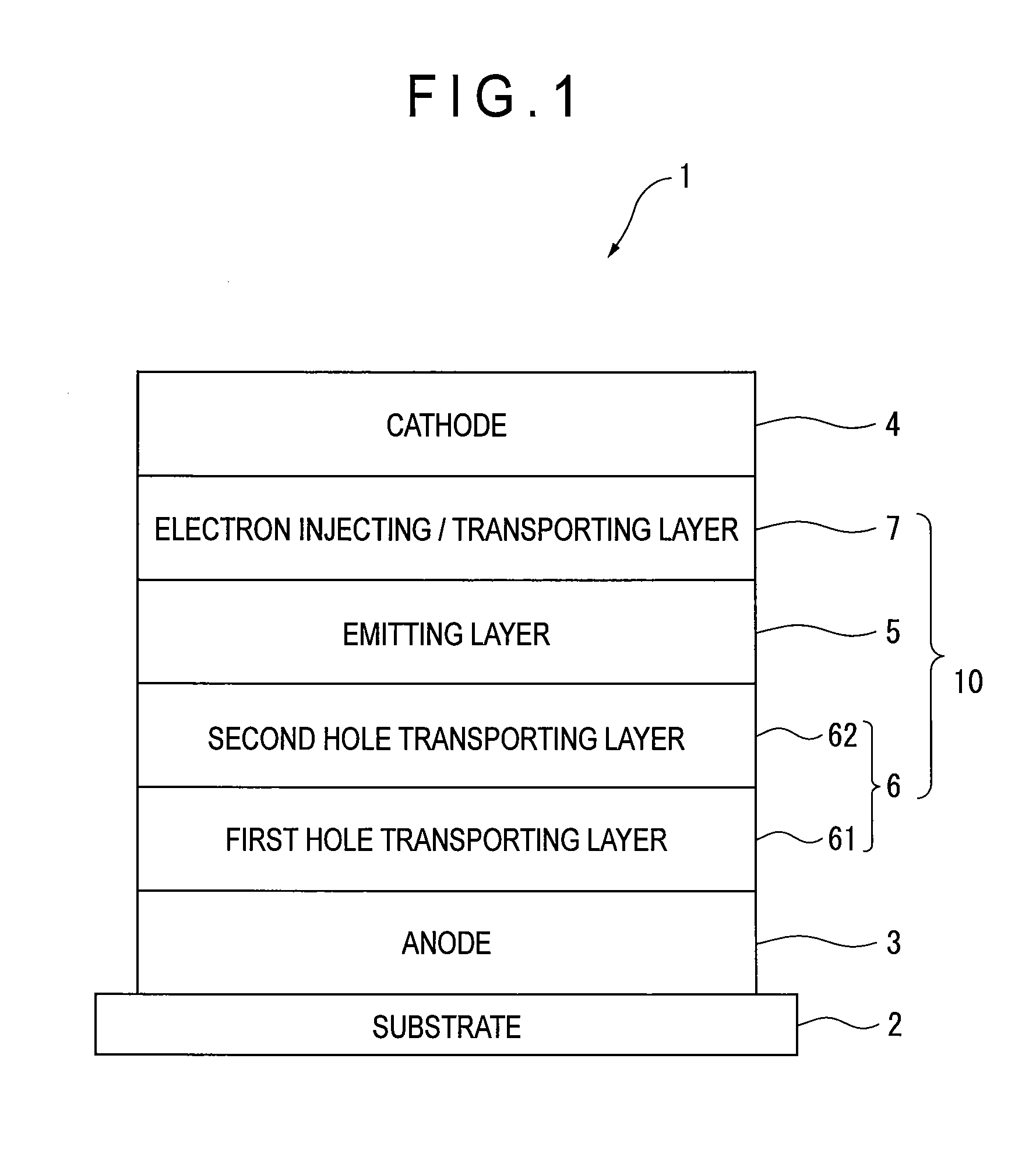
[0166]After the glass substrate having the transparent electrode line was cleaned, the glass substrate was mounted on a substrate holder of a vacuum deposition apparatus, so that an 80-nm thick film of a compound HT0 was initially formed by resistance heating deposition to cover a surface of the glass substrate where the transparent electrode line was provided. This HT0 film serves as the first hole transporting layer.

[0167]After the film-formation of the first hole transporting layer, a 20-nm thick film of an electron-blocking compound HT1 was formed by resistance heating deposition to cover the film of the first hole transporting layer. This HT1 film functions as the second hole transporting layer.

[0168]Further, on the second hole transporting layer,...

examples 2 to 4

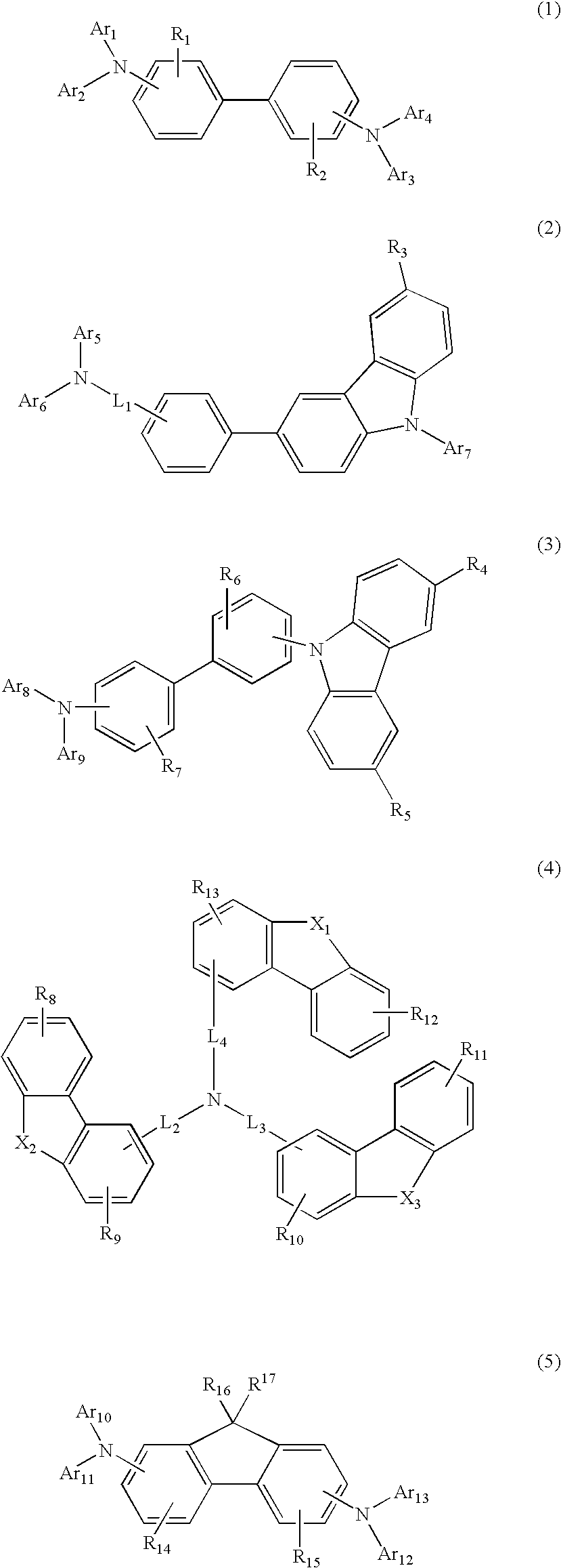
[0171]The organic EL device was manufactured in the same manner as in Example 1 except that HT2, HT3 and HT4 were used in place of HT1 as materials of the second hole transporting layer.

Comparative 1

[0172]The organic EL device was manufactured in the same manner as in Example 1 except that tris(4,4′,4″-(9-carbazolyl))-triphenylamine (TCTA) was used in place of HT1 as materials of the second hole transporting layer.

Comparative 2

[0173]The organic EL device was manufactured in the same manner as in Example 1 except that di(4,4′-(9-carbazolyl))-triphenylamine (DCTA) was used in place of HT1 as materials of the second hole transporting layer.

Comparative 3

[0174]The organic EL device was manufactured in the same manner as in Example 1 except that the hole transporting layer is a 100-nm thick single-layered film of HT3 without laminating the first and second hole transporting layers.

Comparative 4

[0175]The organic EL device was manufactured in the same manner as in Example 1 except that the ...

example 5

[0176]A glass substrate (size: 25 mm×75 mm×1.1 mm thick) having an ITO transparent electrode (manufactured by Asahi Glass Co., Ltd) was ultrasonic-cleaned in isopropyl alcohol for five minutes, and then UV / ozone-cleaned for 30 minutes.

[0177]After the glass substrate having the transparent electrode line was cleaned, the glass substrate was mounted on a substrate holder of a vacuum deposition apparatus, so that 10-nm thick film of a compound HT0 was initially formed by resistance heating deposition to cover a surface of the glass substrate where the transparent electrode line was provided. This HT0 film serves as the first hole transporting layer.

[0178]After the film-formation of the first hole transporting layer, 10-nm thick film of an electron-blocking compound HT4 was formed by resistance heating deposition to cover the film of the first hole transporting layer. This HT4 film serves as the second hole transporting layer.

[0179]Further, on the second hole transporting layer, a compo...


PUM


Abstract

An organic EL device includes: an anode, a cathode and an organic thin-film layer interposed between the anode and the cathode, in which the organic thin-film layer includes: an emitting layer containing a host material and a phosphorescent material; and a hole transporting layer provided adjacent to the anode relative to the emitting layer. The hole transporting layer includes a first hole transporting layer and a second hole transporting layer that are sequentially layered on the anode, in which the first hole transporting layer contains an amino compound substituted by an aromatic substituent represented by a formula (1) below and the second hole transporting layer contains at least one of compounds represented by formulae (2) to (5) below.

Description

CROSS-REFERENCE TO PRIOR APPLICATION[0001]This is the U.S. National Phase Application under 35 U.S.C. §371 of International Patent Application No. PCT / JP2008 / 067523 filed Sep. 26, 2008, which claims the benefit of Japanese Patent Application No. 2007-256308 filed Sep. 28, 2007, both of which are incorporated by reference herein. The International Application was published in Japanese on Apr. 2, 2009 as WO 2009 / 041635 A1 under PCT Article 21(2).TECHNICAL FIELD[0002]The present invention relates to an organic EL device. Particularly, the present invention relates to a phosphorescent organic EL device having high efficiency and long lifetime.BACKGROUND ART[0003]An organic electroluminescent device (hereinafter, electroluminescent is occasionally abbreviated as EL) is a self-emitting device based on the principle that, when an electrical field is applied, a material emits light using energy generated by a recombination of holes injected from an anode with electrons injected from a catho...

Claims


Application Information

Patent Timeline
IPC IPC(8): H01L51/30
CPCH01L51/006H01L51/0061H01L51/0067H01L51/0072C09B57/008H01L51/0081H01L51/5016H01L51/5048C09B57/00H01L51/0073H10K85/636H10K85/633H10K85/654H10K85/6574H10K85/324H10K85/6572H10K50/14H10K50/11H10K2101/10H05B33/20
Inventor ENDO, JUNFUKUOKA, KENICHIIWAKUMA, TOSHIHIROHOSOKAWA, CHISHIOYOSHINAGA, TADAHIKOKAMBE, EMIKOKIJIMA, YASUNORI
Owner IDEMITSU KOSAN CO LTD
Why Eureka
Try Eureka